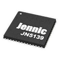
JN5139/001,531 NXP Semiconductors, JN5139/001,531 Datasheet - Page 77

JN5139/001,531
Manufacturer Part Number
JN5139/001,531
Description
MCU 802.15.4 32BIT 2.4G 56-QFN
Manufacturer
NXP Semiconductors
Datasheet
1.JN5139-Z01-V.pdf
(82 pages)
Specifications of JN5139/001,531
Frequency
2.4GHz
Modulation Or Protocol
802.15.4
Applications
General Purpose
Power - Output
*
Sensitivity
-96dBm
Voltage - Supply
2.7 V ~ 3.6 V
Current - Receiving
37mA
Current - Transmitting
37mA
Data Interface
PCB, Surface Mount
Memory Size
96kB RAM, 192kB ROM
Antenna Connector
PCB, Surface Mount
Operating Temperature
-20°C ~ 70°C
Package / Case
56-VFQFN
Core
RISC
Lead Free Status / RoHS Status
Lead free / RoHS Compliant
- Current page: 77 of 82
- Download datasheet (619Kb)
B.2 16MHz Oscillator
The JN5139 contains the necessary on-chip components to build a 16 MHz reference oscillator with the addition of
an external crystal resonator, two tuning capacitors and a resistor. The schematic of these components are shown in
Figure 49. The two capacitors, C1 and C2, will typically be 15pF ±5% and use a COG dielectric, R2 should be 1M5Ω.
For a detailed specification of the crystal required and factors affecting C1 and C2 see Appendix B.1. As with all
crystal oscillators the PCB layout is especially important, both to keep parasitic capacitors to a minimum and to
reduce the possibility of PCB noise being coupled into the oscillator.
The clock generated by this oscillator provides the reference for most of the JN5139 subsystems, including the
transceiver, processor, memory and digital and analogue peripherals.
© NXP Laboratories UK 2010
R2
Crystal Oscillator Transconductance Versus Supply Voltage
XTALIN
1.32
1.28
1.26
1.24
1.22
1.3
1.2
2.2
Figure 49: Crystal oscillator connections
2.4
C1
JN-DS-JN5139 1v9
2.6
(Temp=25C)
R1
Supply Voltage (VDD)
2.8
3.0
C2
XTALOUT
JN5139
3.2
3.4
3.6
77
Related parts for JN5139/001,531
Image
Part Number
Description
Manufacturer
Datasheet
Request
R

Part Number:
Description:
JN5139-Z01-M/SOM041/REEL13 DP
Manufacturer:
NXP Semiconductors
Datasheet:

Part Number:
Description:
JN5139-Z01-M/SOM041/REEL PACK/
Manufacturer:
NXP Semiconductors
Datasheet:

Part Number:
Description:
JN5139-001-M/SOM041/REEL13 DP
Manufacturer:
NXP Semiconductors
Datasheet:

Part Number:
Description:
JN5139-Z01-M/SOM041/REEL13 DP
Manufacturer:
NXP Semiconductors
Datasheet:

Part Number:
Description:
JN5139-Z01-M/SOM041/REEL PACK/
Manufacturer:
NXP Semiconductors
Datasheet:

Part Number:
Description:
JN5139-001-M/SOM041/REEL PACK/
Manufacturer:
NXP Semiconductors
Datasheet:

Part Number:
Description:
JN5139-001-M/SOM041/REEL PACK/
Manufacturer:
NXP Semiconductors
Datasheet:

Part Number:
Description:
JN5139-001-M/SOM041/REEL13 DP
Manufacturer:
NXP Semiconductors
Datasheet:

Part Number:
Description:
JN5139-Z01-M/SOM041/REEL13 DP
Manufacturer:
NXP Semiconductors
Datasheet:

Part Number:
Description:
JN5139-001-M/SOM041/REEL13 DP
Manufacturer:
NXP Semiconductors
Datasheet:

Part Number:
Description:
IC MCU ZIGBEE 32BIT 2.4G 56QFN
Manufacturer:
NXP Semiconductors
Datasheet:

Part Number:
Description:
IC MCU 802.15.4 32BIT 2.4G 56QFN
Manufacturer:
NXP Semiconductors
Datasheet:

Part Number:
Description:
KIT EVAL IEEE802.15.4 JN5139
Manufacturer:
Jennic LTD
Datasheet:

Part Number:
Description:
ZigBee Module W/ Integrated Antenna
Manufacturer:
Jennic LTD
Datasheet:

Part Number:
Description:
32BIT MCU, ZIGBEE, 192K ROM, 5139
Manufacturer:
Jennic LTD
Datasheet:


