EVALA5973AD STMicroelectronics, EVALA5973AD Datasheet - Page 18
EVALA5973AD
Manufacturer Part Number
EVALA5973AD
Description
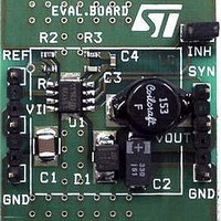
Power Management Modules & Development Tools EVAL BOARD A5973AD Auto Grade
Manufacturer
STMicroelectronics
Type
DC/DC Switching Converters, Regulators & Controllersr
Datasheet
1.EVALA5973D.pdf
(30 pages)
Specifications of EVALA5973AD
Input Voltage
4.4 V to 36 V
Output Voltage
1.235 V to 35 V
Board Size
23 mm x 20 mm
Product
Power Management Modules
Supply Current
2.5 A
Dimensions
23 mm x 20 mm
For Use With/related Products
AN1518
Lead Free Status / RoHS Status
Lead free / RoHS Compliant


Application information
9.3
18/30
High impedance paths (in particular the feedback connections) are susceptible to
interference, so they should be as far as possible from the high current paths. An layout
example is provided in
The input and output loops are minimized to avoid radiation and high frequency resonance
problems. The feedback pin connections to the external divider are very close to the device
to avoid pick-up noise. Another important issue is the groundplane of the board. Since the
package has an exposed pad, it is very important to connect it to an extended groundplane
in order to reduce the thermal resistance junction-to-ambient.
Figure 13. Layout example
Thermal considerations
The dissipated power of the device is tied to three different sources:
●
Equation 22
Where D is the duty cycle of the application. Note that the duty cycle is theoretically given by
the ratio between V
compensate for the losses in the overall application. For this reason, the switching losses
related to the R
●
Equation 23
Switching losses due to the not insignificant R
Switching losses due to turning ON and OFF. These are derived using the following
equation:
VERY SMALL HIGH CURRENT
CIRCULATING PATH TO MINIMIZE
RADIATION AND HIGH FREQUENCY
RESONANCE PROBLEMS
MINIMUN SIZE OF FEEDBACK
PIN CONNECTIONS TO AVOID
PICKUP
P
DSON
SW
OUT
=
CONNECTION TO
GROUNDPLANE
THROUGH VIAS
increase compared to an ideal case.
V
Figure 13
IN
and V
•
I
R2
OUT
R1
to output voltage
IN
Cin
Vin
, but in practice it is substantially higher than this value to
•
P
below.
(
----------------------------------- -
ON
T
5
8
ON
L5973D
=
+
2
R
T
DSON
OFF
4
1
)
Inhibit signal
•
•
(
F
D
I
COMPENSATION NETWORK FAR
FROM HIGH CURRENT PATHS
OUT
SW
DSON
=
)
2
V
•
, which are equal to:
IN
Cout
L
D
•
I
OUT
Vout
Gnd
•
T
SW
OUTPUT CAPACITOR
DIRECTLY
CONNECTED TO
HEAVY GROUND
EXTENDED GROUNDPLANE
ON THE BOTTOM SIDE
•
F
SW
AN1518
Related parts for EVALA5973AD
Image
Part Number
Description
Manufacturer
Datasheet
Request
R

Part Number:
Description:
ENERCHIP CC EVAL KIT
Manufacturer:
Cymbet Corporation
Datasheet:

Part Number:
Description:
BOARD EVAL FOR AD976
Manufacturer:
Analog Devices Inc
Datasheet:

Part Number:
Description:
BOARD EVAL FOR ADXL345
Manufacturer:
Analog Devices Inc
Datasheet:

Part Number:
Description:
ENERCHIP CC SEH EVAL KIT
Manufacturer:
Cymbet Corporation
Datasheet:

Part Number:
Description:
ENERCHIP EP ENERGY HARVEST EVAL
Manufacturer:
Cymbet Corporation
Datasheet:

Part Number:
Description:
EVAL BOARD FOR TW6864-LB2-GR
Manufacturer:
Intersil
Datasheet:
Part Number:
Description:
EVAL BOARD FOR TW8816-LB3-GR
Manufacturer:
Intersil
Datasheet:
Part Number:
Description:
EVAL BOARD FOR TW8817-TA3-GRS
Manufacturer:
Intersil
Datasheet:

Part Number:
Description:
EVALUATION MODULE FOR ADUM4160
Manufacturer:
Analog Devices Inc
Datasheet:

Part Number:
Description:
BOARD EVALUATION ADCMP581BCP
Manufacturer:
Analog Devices Inc
Datasheet:
Part Number:
Description:
BOARD EVALUATION ADM1041
Manufacturer:
Analog Devices Inc
Datasheet:

Part Number:
Description:
EVAL BOARD FOR STM32F107VCT
Manufacturer:
STMicroelectronics
Datasheet:
Part Number:
Description:
BOARD EVAL FOR AD1954
Manufacturer:
Analog Devices Inc
Datasheet:
Part Number:
Description:
BOARD EVAL FOR AD1955
Manufacturer:
Analog Devices Inc
Datasheet:

Part Number:
Description:
BOARD EVAL FOR AD7655
Manufacturer:
Analog Devices Inc
Datasheet: