EVALA5973AD STMicroelectronics, EVALA5973AD Datasheet - Page 7
EVALA5973AD
Manufacturer Part Number
EVALA5973AD
Description
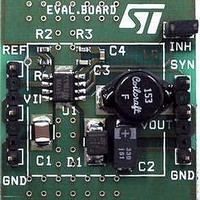
Power Management Modules & Development Tools EVAL BOARD A5973AD Auto Grade
Manufacturer
STMicroelectronics
Type
DC/DC Switching Converters, Regulators & Controllersr
Datasheet
1.EVALA5973D.pdf
(30 pages)
Specifications of EVALA5973AD
Input Voltage
4.4 V to 36 V
Output Voltage
1.235 V to 35 V
Board Size
23 mm x 20 mm
Product
Power Management Modules
Supply Current
2.5 A
Dimensions
23 mm x 20 mm
For Use With/related Products
AN1518
Lead Free Status / RoHS Status
Lead free / RoHS Compliant


AN1518
3.3
3.4
Oscillator & synchronizer
Figure 6
The Clock Generator provides the switching frequency of the device, which is internally fixed
at 250 kHz. The Frequency Shifter block acts to reduce the switching frequency in case of
strong overcurrent or short circuit. The clock signal is then used in the internal logic circuitry
and is the input of the Ramp Generator and Synchronizer blocks.
The Ramp Generator circuit provides the sawtooth signal, used for PWM control and
internal voltage feed-forward, while the synchronizer circuit generates the synchronization
signal. The device also has a synchronization pin which can work both as Master and Slave.
As Master, it serves to synchronize external devices to the internal switching frequency, and
as Slave to synchronize itself using an external signal up to 500 kHz.
In particular, when connecting together two devices the one with the lower switching
frequency works as a Slave and the other as Master.
To synchronize the device, the SYNC pin must pass from a low level to a level higher than
the synchronization threshold with a duty cycle that can vary from approximately 10% to
90%, depending also on the signal frequency and amplitude.
The frequency of the synchronization signal must be, at a minimum, higher than the internal
switching frequency of the device (250 kHz).
Figure 6.
Current protection
The L5973D features two types of current limit protection: pulse-by-pulse and frequency
foldback.
The schematic of the current limitation circuitry for the pulse-by-pulse protection is shown in
Figure
The smallest one includes a resistor in series, R
R
switched off until the next falling edge of the internal clock pulse. Due to this reduction of the
ON time, the output voltage decreases. Since the minimum switch ON time (necessary to
avoid false a overcurrent signal) is too short to obtain a sufficiently low duty cycle at 250
kHz, the output current, in strong overcurrent or short circuit conditions, could increase
SENSE
7. The output power PDMOS transistor is split into two parallel PDMOS transistors.
and if it reaches the threshold, the mirror becomes unbalanced and the PDMOS is
shows the block diagram of the oscillator circuit.
Oscillator circuit block diagram
SENSE
. The current is sensed through
Functional description
7/30
Related parts for EVALA5973AD
Image
Part Number
Description
Manufacturer
Datasheet
Request
R

Part Number:
Description:
ENERCHIP CC EVAL KIT
Manufacturer:
Cymbet Corporation
Datasheet:

Part Number:
Description:
BOARD EVAL FOR AD976
Manufacturer:
Analog Devices Inc
Datasheet:

Part Number:
Description:
BOARD EVAL FOR ADXL345
Manufacturer:
Analog Devices Inc
Datasheet:

Part Number:
Description:
ENERCHIP CC SEH EVAL KIT
Manufacturer:
Cymbet Corporation
Datasheet:

Part Number:
Description:
ENERCHIP EP ENERGY HARVEST EVAL
Manufacturer:
Cymbet Corporation
Datasheet:

Part Number:
Description:
EVAL BOARD FOR TW6864-LB2-GR
Manufacturer:
Intersil
Datasheet:
Part Number:
Description:
EVAL BOARD FOR TW8816-LB3-GR
Manufacturer:
Intersil
Datasheet:
Part Number:
Description:
EVAL BOARD FOR TW8817-TA3-GRS
Manufacturer:
Intersil
Datasheet:

Part Number:
Description:
EVALUATION MODULE FOR ADUM4160
Manufacturer:
Analog Devices Inc
Datasheet:

Part Number:
Description:
BOARD EVALUATION ADCMP581BCP
Manufacturer:
Analog Devices Inc
Datasheet:
Part Number:
Description:
BOARD EVALUATION ADM1041
Manufacturer:
Analog Devices Inc
Datasheet:

Part Number:
Description:
EVAL BOARD FOR STM32F107VCT
Manufacturer:
STMicroelectronics
Datasheet:
Part Number:
Description:
BOARD EVAL FOR AD1954
Manufacturer:
Analog Devices Inc
Datasheet:
Part Number:
Description:
BOARD EVAL FOR AD1955
Manufacturer:
Analog Devices Inc
Datasheet:

Part Number:
Description:
BOARD EVAL FOR AD7655
Manufacturer:
Analog Devices Inc
Datasheet: