VNCLO-PSU-USA FTDI, Future Technology Devices International Ltd, VNCLO-PSU-USA Datasheet - Page 5
VNCLO-PSU-USA
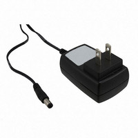
Manufacturer Part Number
VNCLO-PSU-USA
Description
POWER SUPPLY FOR VNCLO-MB1A USA
Manufacturer
FTDI, Future Technology Devices International Ltd
Series
Vinculor
Specifications of VNCLO-PSU-USA
Accessory Type
Power Supply
Lead Free Status / RoHS Status
Lead free / RoHS Compliant
For Use With/related Products
FTDI Vinculo Boards
Other names
768-1092


2
This block diagram, Figure 2.1, shows the interconnect required for the Vinco to drive the LCD display.
The Vinco debug port is used to load the firmware onto the module. (Note that this requires a VNC2
DEBUG MODULE
)
The interconnect between the two modules is used to transfer the text to be displayed on the LCD.
Figure 2.1 – Vinco Sign Writer Demo Block Diagram
Block Diagram
VINCO
CN1
J8
DEBUG PORT
+9V DC POWER
ADAPTER
http://ftdichip.com/Support/Documents/DataSheets/Modules/DS_V2Debug_Module.pdf
J3-2
J3-1
J3-3
J3-4
J3-5
J3-6
J1-5
J1-6
Copyright © 2010 Future Technology Devices International Limited
`
GND
DB4
DB5
DB6
DB7
RS
5V
E
11
12
13
14
4
6
2
1
16 CHAR x 2 LINE
LCD DISPLAY
TOPWAY
10k
10
3
7
8
9
R/W
BLA
BLK
AN_153 Vinco LCD Interface Example
V0 – CONTRAST
CONTROL
Document Reference No.: FT_000332
UNUSED DB0-DB3
GND
GND
5V
Clearance No.: FTDI# 177
(ONLY WRITING)
BACKLIGHT
Version
4
2.0
Related parts for VNCLO-PSU-USA
Image
Part Number
Description
Manufacturer
Datasheet
Request
R

Part Number:
Description:
POWER SUPPLY FOR VNCLO-MB1A EU
Manufacturer:
FTDI, Future Technology Devices International Ltd
Datasheet:
Part Number:
Description:
POWER SUPPLY FOR VNCLO-MB1A UK
Manufacturer:
FTDI, Future Technology Devices International Ltd
Datasheet:

Part Number:
Description:
Interface Modules & Development Tools Vinculo Motherboard Req VNC2DEBUGMODULE
Manufacturer:
FTDI
Datasheet:

Part Number:
Description:
Interface Modules & Development Tools Vinculo Prototyping Shield Accessory
Manufacturer:
FTDI
Datasheet:
Part Number:
Description:
KIT, DEV, VINCULUM-II, VNC2
Manufacturer:
FTDI
Datasheet:

Part Number:
Description:
IC USB TO SERIAL UART 32-QFN
Manufacturer:
FTDI, Future Technology Devices International Ltd

Part Number:
Description:
IC USB HOST CTLR VINCULUM 48LQFP
Manufacturer:
FTDI, Future Technology Devices International Ltd
Datasheet:

Part Number:
Description:
IC USB HOST VINCULUM-II 32QFN
Manufacturer:
FTDI, Future Technology Devices International Ltd
Datasheet:
Part Number:
Description:
IC USB HOST VINCULUM-II 32LQFN
Manufacturer:
FTDI, Future Technology Devices International Ltd
Datasheet:
Part Number:
Description:
IC USB HOST VINCULUM-II 48QFN
Manufacturer:
FTDI, Future Technology Devices International Ltd
Datasheet:
Part Number:
Description:
IC USB HOST VINCULUM-II 32LQFN
Manufacturer:
FTDI, Future Technology Devices International Ltd
Datasheet:
Part Number:
Description:
IC USB HOST VINCULUM-II 32QFN
Manufacturer:
FTDI, Future Technology Devices International Ltd
Datasheet:
Part Number:
Description:
IC USB HOST VINCULUM-II 48LQFP
Manufacturer:
FTDI, Future Technology Devices International Ltd
Datasheet:
Part Number:
Description:
IC USB HOST VINCULUM-II 48LQFP
Manufacturer:
FTDI, Future Technology Devices International Ltd
Datasheet:
Part Number:
Description:
IC USB HOST VINCULUM-II 48QFN
Manufacturer:
FTDI, Future Technology Devices International Ltd
Datasheet: