VNCLO-PSU-USA FTDI, Future Technology Devices International Ltd, VNCLO-PSU-USA Datasheet - Page 7
VNCLO-PSU-USA
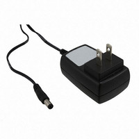
Manufacturer Part Number
VNCLO-PSU-USA
Description
POWER SUPPLY FOR VNCLO-MB1A USA
Manufacturer
FTDI, Future Technology Devices International Ltd
Series
Vinculor
Specifications of VNCLO-PSU-USA
Accessory Type
Power Supply
Lead Free Status / RoHS Status
Lead free / RoHS Compliant
For Use With/related Products
FTDI Vinculo Boards
Other names
768-1092


3.3 Debugger Interface
The purpose of the debugger interface is to provide access to the VNC2 silicon/firmware debugger. The
debug interface can be accessed by connecting a VNC2_Debug_Module
(http://www.ftdichip.com/Support/Documents/DataSheets/ICs/DS_Vinculum-II.pdf
This debug module gives access to the debugger through a USB connection to a PC via the Integrated
Development Environment (IDE). The IDE is a graphical interface to the VNC2 software development
tool-chain and gives the following debug capabilities through the debugger interface:
The IDE may be downloaded, free of charge, from
http://www.ftdichip.com/Firmware/V2TC/VNC2toolchain.htm
The Debugger Interface, and how to use it, is further described in the following applications Note
Vinculum-II Debug Interface Description
Table 3.2 shows the signals and pins description for the Debugger Interface pin header J8
J8-1
J8-2
J8-3
J8-4
J8-5
J8-6
Table 3.2 - Signal Name and Description – Debugger Interface
Pin No.
3.3.1 Signal Description - Debugger Interface
Flash Erase, Write and Program.
Application debug - application code can have breakpoints, be single stepped and can be halted.
Detailed internal debug - memory and register read/write access.
RESET#
PROG#
Name
GND
IO0
5V0
-
Copyright © 2010 Future Technology Devices International Limited
On PCB
Name
`
PRG#
[Key]
RST#
DBG
GND
VCC
PWR Input
Type
Input
Input
PWR
I/O
-
Can be used by an external device to reset the
VNCL2. This pin is also used in combination with
PROG# and the UART interface to program
firmware into the VNC2.
This pin is used in combination with the RESET#
pin and the UART interface to program firmware
into the VNC2.
5.0V module supply pin. This pin can be used to
provide the 5.0V input to the V2DIP2-32 from the
debugger interface when the V2DIP2-32 is not
powered from the USB connector (VBUs) or the
DIL connector pins J1-1 and J3-6.
Not connected. Used to make sure that the debug
module is connected correctly.
Module ground supply pin
AN_153 Vinco LCD Interface Example
Debugger Interface
Description
Document Reference No.: FT_000332
Clearance No.: FTDI# 177
) to the J8 connector.
Version
6
2.0
Related parts for VNCLO-PSU-USA
Image
Part Number
Description
Manufacturer
Datasheet
Request
R

Part Number:
Description:
POWER SUPPLY FOR VNCLO-MB1A EU
Manufacturer:
FTDI, Future Technology Devices International Ltd
Datasheet:
Part Number:
Description:
POWER SUPPLY FOR VNCLO-MB1A UK
Manufacturer:
FTDI, Future Technology Devices International Ltd
Datasheet:

Part Number:
Description:
Interface Modules & Development Tools Vinculo Motherboard Req VNC2DEBUGMODULE
Manufacturer:
FTDI
Datasheet:

Part Number:
Description:
Interface Modules & Development Tools Vinculo Prototyping Shield Accessory
Manufacturer:
FTDI
Datasheet:
Part Number:
Description:
KIT, DEV, VINCULUM-II, VNC2
Manufacturer:
FTDI
Datasheet:

Part Number:
Description:
IC USB TO SERIAL UART 32-QFN
Manufacturer:
FTDI, Future Technology Devices International Ltd

Part Number:
Description:
IC USB HOST CTLR VINCULUM 48LQFP
Manufacturer:
FTDI, Future Technology Devices International Ltd
Datasheet:

Part Number:
Description:
IC USB HOST VINCULUM-II 32QFN
Manufacturer:
FTDI, Future Technology Devices International Ltd
Datasheet:
Part Number:
Description:
IC USB HOST VINCULUM-II 32LQFN
Manufacturer:
FTDI, Future Technology Devices International Ltd
Datasheet:
Part Number:
Description:
IC USB HOST VINCULUM-II 48QFN
Manufacturer:
FTDI, Future Technology Devices International Ltd
Datasheet:
Part Number:
Description:
IC USB HOST VINCULUM-II 32LQFN
Manufacturer:
FTDI, Future Technology Devices International Ltd
Datasheet:
Part Number:
Description:
IC USB HOST VINCULUM-II 32QFN
Manufacturer:
FTDI, Future Technology Devices International Ltd
Datasheet:
Part Number:
Description:
IC USB HOST VINCULUM-II 48LQFP
Manufacturer:
FTDI, Future Technology Devices International Ltd
Datasheet:
Part Number:
Description:
IC USB HOST VINCULUM-II 48LQFP
Manufacturer:
FTDI, Future Technology Devices International Ltd
Datasheet:
Part Number:
Description:
IC USB HOST VINCULUM-II 48QFN
Manufacturer:
FTDI, Future Technology Devices International Ltd
Datasheet: