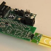
MC33696MOD868EV Freescale Semiconductor, MC33696MOD868EV Datasheet - Page 23

MC33696MOD868EV
Manufacturer Part Number
MC33696MOD868EV
Description
MCU, MPU & DSP Development Tools MC33696 (ECHO) RF C EVAL
Manufacturer
Freescale Semiconductor
Datasheet
1.MC33696MOD868EV.pdf
(80 pages)
Specifications of MC33696MOD868EV
Processor To Be Evaluated
MC9S08RG60
Interface Type
RS-232
Lead Free Status / RoHS Status
Lead free / RoHS Compliant
Each time is defined with the associated value found in the RXONOFF register.
The strobe oscillator is a relaxation oscillator in which an external capacitor C13 is charged by an internal
current source (see
The strobe frequency is F
In receive mode, setting the STROBE pin to V
the oscillator threshold voltage, the condition on which the STROBE pin is set to V
internally, and the oscillator pulldown circuitry is disabled. This limits the current consumption. After the
STROBE pin is forced to high level, the external driver should pass via a “0” state to discharge the
capacitor before going to high impedance state (otherwise, the on time would last a long time after the
driver release).
When the strobe oscillator is running (i.e., during an off time), forcing the STROBE pin to V
strobe clock, and therefore keeps the circuit off.
Figure 14
12.4 Received Signal Strength Indicator (RSSI)
12.4.1 Module Description
In receive mode, a received signal strength indicator can be activated by setting bit RSSIE.
The input signal is measured at two different points in the receiver chain by two different means, as
follows.
Freescale Semiconductor
•
•
•
STROBE
STROBE
On time = RON[3:0] × 512 × T
Off time = receiver off time = N × T
from ROFF[2:0] (see
Receiver
At the IF filter output, a progressive compression logarithmic amplifier measures the input signal,
ranging from the sensitivity level up to –50 dBm.
Counter
Counter
Status
Digital
Clock
Clock
shows the associated timings.
Off
On
Threshold
0
RON
Figure
Strobe
46). When the threshold is reached, C13 is discharged and the cycle restarts.
Off
Table
Cycling Period
0
t
Strobe
= 1/T
ROFF-1 ROFF
Figure 14. Receiver On/Off Sequence
20)
Strobe
digclk
MC33696 Data Sheet, Rev. 12
with T
Strobe
(see
On
CCIO
Crystal Oscillator Startup
0
Table
Strobe
+ MIN (T
RON
at any time forces the circuit on. As V
= 10
19; begins after the crystal oscillator has started)
Off
Strobe
6
0
× C13.
/ 2, receiver on time), with N decoded
SET TO V
STROBE
RON
On
CCIO
CCIO
is detected
CCIO
GND
Receive Mode
is above
stops the
23


