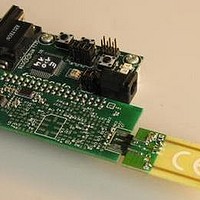
MC33696MOD868EV Freescale Semiconductor, MC33696MOD868EV Datasheet - Page 36

MC33696MOD868EV
Manufacturer Part Number
MC33696MOD868EV
Description
MCU, MPU & DSP Development Tools MC33696 (ECHO) RF C EVAL
Manufacturer
Freescale Semiconductor
Datasheet
1.MC33696MOD868EV.pdf
(80 pages)
Specifications of MC33696MOD868EV
Processor To Be Evaluated
MC9S08RG60
Interface Type
RS-232
Lead Free Status / RoHS Status
Lead free / RoHS Compliant
- Current page: 36 of 80
- Download datasheet (2Mb)
Register Description
The change of duration of one state (due to the STROBE pin level or a message being received) has no
influence on the timing of the following states (A, B, or OFF).
18
This section discusses the internal registers, which are composed of two classes of bits.
All registers can be accessed by the SPI. These registers are described below.
At power-on, the POR resets all registers to a known value (in the shaded rows in the following tables).
This defines the MC33696’s default configuration.
18.1 Configuration Registers (Description Bank A only)
Figure 25
RESET is a global reset. The bit is cleared internally, after use.
SL (Switch Level) selects the active level of the SWITCH output pin.
36
Reset Value
Bit Name
•
•
•
•
Access
If strobe pin is 0 the state is OFF.
If strobe pin is released from 0 while state is OFF, the initial OFF period is completed.
Configuration and command bits allow the MC33696 to operate in a suitable configuration.
Status bits report the current state of the system.
0 = no action
1 = reset all registers and counters
Register Description
describes configuration register 1, CONFIG1.
LOF1
Bit 7
R/W
1
Carrier Frequency
Table 8. LOF[1:0] and CF[1:0] Setting Versus Carrier Frequency
304 MHz
315 MHz
426 MHz
434 MHz
868 MHz
915 MHz
LOF0
Bit 6
R/W
0
Bit 5
CF1
R/W
Figure 25. CONFIG1 Register
0
MC33696 Data Sheet, Rev. 12
LOF1
0
1
0
0
0
1
Bit 4
CF0
R/W
1
RESET
LOF0
Bit 3
R/W
0
0
1
1
1
1
0
Bit 2
R/W
CF1
SL
0
0
0
0
0
1
1
LVDE
Bit 1
R/W
0
CF0
0
0
1
1
1
1
Freescale Semiconductor
CLKE
Bit 0
R/W
1
Addr
$00
Related parts for MC33696MOD868EV
Image
Part Number
Description
Manufacturer
Datasheet
Request
R
Part Number:
Description:
Manufacturer:
Freescale Semiconductor, Inc
Datasheet:
Part Number:
Description:
Manufacturer:
Freescale Semiconductor, Inc
Datasheet:
Part Number:
Description:
Manufacturer:
Freescale Semiconductor, Inc
Datasheet:
Part Number:
Description:
Manufacturer:
Freescale Semiconductor, Inc
Datasheet:
Part Number:
Description:
Manufacturer:
Freescale Semiconductor, Inc
Datasheet:
Part Number:
Description:
Manufacturer:
Freescale Semiconductor, Inc
Datasheet:
Part Number:
Description:
Manufacturer:
Freescale Semiconductor, Inc
Datasheet:
Part Number:
Description:
Manufacturer:
Freescale Semiconductor, Inc
Datasheet:
Part Number:
Description:
Manufacturer:
Freescale Semiconductor, Inc
Datasheet:
Part Number:
Description:
Manufacturer:
Freescale Semiconductor, Inc
Datasheet:
Part Number:
Description:
Manufacturer:
Freescale Semiconductor, Inc
Datasheet:
Part Number:
Description:
Manufacturer:
Freescale Semiconductor, Inc
Datasheet:
Part Number:
Description:
Manufacturer:
Freescale Semiconductor, Inc
Datasheet:
Part Number:
Description:
Manufacturer:
Freescale Semiconductor, Inc
Datasheet:
Part Number:
Description:
Manufacturer:
Freescale Semiconductor, Inc
Datasheet:


