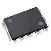
C8051F124TB Silicon Laboratories Inc, C8051F124TB Datasheet - Page 245

C8051F124TB
Manufacturer Part Number
C8051F124TB
Description
MCU, MPU & DSP Development Tools With C8051F124 MCU
Manufacturer
Silicon Laboratories Inc
Datasheet
1.C8051F120DK.pdf
(350 pages)
Specifications of C8051F124TB
Processor To Be Evaluated
C8051F12x and C8051F13x
Interface Type
USB
Lead Free Status / RoHS Status
Lead free / RoHS Compliant
- Current page: 245 of 350
- Download datasheet (2Mb)
Bit7:
Bit6:
Bits5–3: PCA0ME: PCA0 Module I/O Enable Bits.
Bit2:
Bit1:
Bit0:
CP0E
R/W
Bit7
CP0E: Comparator 0 Output Enable Bit.
0: CP0 unavailable at Port pin.
1: CP0 routed to Port pin.
ECI0E: PCA0 External Counter Input Enable Bit.
0: PCA0 External Counter Input unavailable at Port pin.
1: PCA0 External Counter Input (ECI0) routed to Port pin.
000: All PCA0 I/O unavailable at port pins.
001: CEX0 routed to port pin.
010: CEX0, CEX1 routed to 2 port pins.
011: CEX0, CEX1, and CEX2 routed to 3 port pins.
100: CEX0, CEX1, CEX2, and CEX3 routed to 4 port pins.
101: CEX0, CEX1, CEX2, CEX3, and CEX4 routed to 5 port pins.
110: CEX0, CEX1, CEX2, CEX3, CEX4, and CEX5 routed to 6 port pins.
UART0EN: UART0 I/O Enable Bit.
0: UART0 I/O unavailable at Port pins.
1: UART0 TX routed to P0.0, and RX routed to P0.1.
SPI0EN: SPI0 Bus I/O Enable Bit.
0: SPI0 I/O unavailable at Port pins.
1: SPI0 SCK, MISO, MOSI, and NSS routed to 4 Port pins. Note that the NSS signal is not
assigned to a port pin if the SPI is in 3-wire mode. See Section “
Interface and On-Chip XRAM
SMB0EN: SMBus0 Bus I/O Enable Bit.
0: SMBus0 I/O unavailable at Port pins.
1: SMBus0 SDA and SCL routed to 2 Port pins.
ECI0E
SFR Definition 18.1. XBR0: Port I/O Crossbar Register 0
R/W
Bit6
R/W
Bit5
PCA0ME
R/W
Bit4
” on page
Rev. 1.4
R/W
Bit3
219
C8051F120/1/2/3/4/5/6/7
for more information.
UART0EN SPI0EN
R/W
Bit2
C8051F130/1/2/3
R/W
Bit1
17. External Data Memory
SFR Address:
SMB0EN 00000000
SFR Page:
R/W
Bit0
0xE1
F
Reset Value
245
Related parts for C8051F124TB
Image
Part Number
Description
Manufacturer
Datasheet
Request
R
Part Number:
Description:
SMD/C°/SINGLE-ENDED OUTPUT SILICON OSCILLATOR
Manufacturer:
Silicon Laboratories Inc
Part Number:
Description:
Manufacturer:
Silicon Laboratories Inc
Datasheet:
Part Number:
Description:
N/A N/A/SI4010 AES KEYFOB DEMO WITH LCD RX
Manufacturer:
Silicon Laboratories Inc
Datasheet:
Part Number:
Description:
N/A N/A/SI4010 SIMPLIFIED KEY FOB DEMO WITH LED RX
Manufacturer:
Silicon Laboratories Inc
Datasheet:
Part Number:
Description:
N/A/-40 TO 85 OC/EZLINK MODULE; F930/4432 HIGH BAND (REV E/B1)
Manufacturer:
Silicon Laboratories Inc
Part Number:
Description:
EZLink Module; F930/4432 Low Band (rev e/B1)
Manufacturer:
Silicon Laboratories Inc
Part Number:
Description:
I°/4460 10 DBM RADIO TEST CARD 434 MHZ
Manufacturer:
Silicon Laboratories Inc
Part Number:
Description:
I°/4461 14 DBM RADIO TEST CARD 868 MHZ
Manufacturer:
Silicon Laboratories Inc
Part Number:
Description:
I°/4463 20 DBM RFSWITCH RADIO TEST CARD 460 MHZ
Manufacturer:
Silicon Laboratories Inc
Part Number:
Description:
I°/4463 20 DBM RADIO TEST CARD 868 MHZ
Manufacturer:
Silicon Laboratories Inc
Part Number:
Description:
I°/4463 27 DBM RADIO TEST CARD 868 MHZ
Manufacturer:
Silicon Laboratories Inc
Part Number:
Description:
I°/4463 SKYWORKS 30 DBM RADIO TEST CARD 915 MHZ
Manufacturer:
Silicon Laboratories Inc
Part Number:
Description:
N/A N/A/-40 TO 85 OC/4463 RFMD 30 DBM RADIO TEST CARD 915 MHZ
Manufacturer:
Silicon Laboratories Inc
Part Number:
Description:
I°/4463 20 DBM RADIO TEST CARD 169 MHZ
Manufacturer:
Silicon Laboratories Inc


