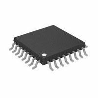
AD7265BSUZ Analog Devices Inc, AD7265BSUZ Datasheet - Page 22

AD7265BSUZ
Manufacturer Part Number
AD7265BSUZ
Description
IC,Data Acquisition System,3-CHANNEL,12-BIT,TQFP,32PIN,PLASTIC
Manufacturer
Analog Devices Inc
Datasheet
1.AD7265BCPZ-REEL.pdf
(28 pages)
Specifications of AD7265BSUZ
Design Resources
AD7265 in Differential and Single-Ended Configurations Using AD8022 (CN0048)
Number Of Bits
12
Sampling Rate (per Second)
1M
Data Interface
DSP, MICROWIRE™, QSPI™, Serial, SPI™
Number Of Converters
2
Power Dissipation (max)
21mW
Voltage Supply Source
Analog and Digital
Operating Temperature
-40°C ~ 125°C
Mounting Type
Surface Mount
Package / Case
32-TQFP, 32-VQFP
Number Of Elements
2
Resolution
12Bit
Architecture
SAR
Sample Rate
1MSPS
Input Polarity
Unipolar
Input Type
Voltage
Rated Input Volt
2.5/5V
Differential Input
Yes
Power Supply Requirement
Analog and Digital
Single Supply Voltage (typ)
3/5V
Single Supply Voltage (min)
2.7V
Single Supply Voltage (max)
5.25V
Dual Supply Voltage (typ)
Not RequiredV
Dual Supply Voltage (min)
Not RequiredV
Dual Supply Voltage (max)
Not RequiredV
Power Dissipation
21mW
Differential Linearity Error
-0.99LSB/1.5LSB
Integral Nonlinearity Error
±1.5LSB
Operating Temp Range
-40C to 125C
Operating Temperature Classification
Automotive
Mounting
Surface Mount
Pin Count
32
Package Type
TQFP
Lead Free Status / RoHS Status
Lead free / RoHS Compliant
For Use With
EVAL-AD7265CB - BOARD EVALUATION FOR AD7265
Lead Free Status / Rohs Status
Compliant
Available stocks
Company
Part Number
Manufacturer
Quantity
Price
Company:
Part Number:
AD7265BSUZ
Manufacturer:
ADI
Quantity:
200
Company:
Part Number:
AD7265BSUZ
Manufacturer:
Analog Devices Inc
Quantity:
10 000
Company:
Part Number:
AD7265BSUZ-REEL
Manufacturer:
Analog Devices Inc
Quantity:
10 000
Company:
Part Number:
AD7265BSUZ-REEL7
Manufacturer:
Analog Devices Inc
Quantity:
10 000
Part Number:
AD7265BSUZ-REEL7
Manufacturer:
ADI/亚德诺
Quantity:
20 000
AD7265
SERIAL INTERFACE
Figure 41 shows the detailed timing diagram for serial inter-
facing to the AD7265. The serial clock provides the conversion
clock and controls the transfer of information from the AD7265
during conversion.
The
The falling edge of CS puts the track-and-hold into hold mode,
at which point the analog input is sampled and the bus is taken
out of three-state. The conversion is also initiated at this point
and requires a minimum of 14 SCLKs to complete. Once 13
SCLK falling edges have elapsed, the track-and-hold goes back
into track on the next SCLK rising edge, as shown in
at Point B. If a 16-SCLK transfer is used, then two trailing zeros
will appear after the final LSB. On the rising edge of
conversion is terminated and D
three-state. If
a further 14 (or 16) SCLK cycles on D
version B is output on D
Likewise, if
on D
is illustrated in Figure 42 where the case for D
this case, the D
32
occurs first.
nd
CS
SCLK falling edge or the rising edge of CS , whichever
OUT
signal initiates the data transfer and conversion process.
B, the data from Conversion A is output on D
D
SCLK
OUT
D
D
SCLK
CS
OUT
OUT
CS
A
CS
CS is not brought high but is instead held low for
THREE-
STATE
A
B
OUT
is held low for a further 14 (or 16) SCLK cycles
THREE-
STATE
line in use goes back into three-state on the
t
2
2 LEADING
0
2 LEADING ZEROS
ZEROS
1
t
OUT
2
ZERO
t
0
3
1
A (followed by 2 trailing zeros).
t
3
0
2
DB11
OUT
A and D
2
A
DB11
3
OUT
DB10
Figure 42. Reading Data from Both ADCs on One D
A, the data from Con-
A
3
OUT
DB10
4
DB9
OUT
B go back into
t
t
6
A
4
A is shown. In
4
t
Figure 41. Serial Interface Timing Diagram
5
5
CS , the
DB9
Figure 41
OUT
t
t
6
4
B. This
2 TRAILING ZEROS
t
5
14
7
ZERO
Rev. A | Page 22 of 28
DB8
t
7
15
ZERO
2 LEADING ZEROS
16
A minimum of 14 serial clock cycles are required to perform
the conversion process and to access data from one conversion
on either data line of the AD7265.
leading zero to be read in by the microcontroller or DSP. The
remaining data is then clocked out by subsequent SCLK falling
edges, beginning with a second leading zero. Therefore, the first
falling clock edge on the serial clock has the leading zero pro-
vided and also clocks out the second leading zero. The 12-bit
result then follows with the final bit in the data transfer valid on
the 14
(13
each SCLK rising edge depending on the SCLK frequency or
the supply voltage. The first rising edge of SCLK after the
falling edge would have the second leading zero provided, and
the 13
Note that with fast SCLK values, and thus short SCLK periods,
in order to allow adequately for t
occur before the first SCLK falling edge. This rising edge of
SCLK can be ignored for the purposes of the timing descriptions in
this section. If a falling edge of SCLK is coincident with the
falling edge of
acknowledged by the AD7265, and the next falling edge of
SCLK will be the first registered after the falling edge of
ZERO
DB2
th
) falling edge. It may also be possible to read in data on
th
th
17
ZERO
OUT
falling edge, having being clocked out on the previous
rising SCLK edge would have DB0 provided.
t
5
Line with 32 SCLKs
DB1
DB11
CS , then this falling edge of SCLK is not
13
B
B
t
DB0
8
ZERO
THREE-STATE
2 TRAILING ZEROS
2
t
, an SCLK rising edge may
QUIET
CS going low provides the
ZERO
t
9
32
t
10
THREE-
STATE
CS .
CS


