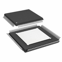
AD9272BSVZRL-65 Analog Devices Inc, AD9272BSVZRL-65 Datasheet - Page 23

AD9272BSVZRL-65
Manufacturer Part Number
AD9272BSVZRL-65
Description
12Bit 65 MSPS Octal ADC
Manufacturer
Analog Devices Inc
Type
Ultrasound Receiversr
Datasheet
1.AD9272BSVZ-80.pdf
(44 pages)
Specifications of AD9272BSVZRL-65
Design Resources
Powering AD9272 with ADP5020 Switching Regulator PMU for Increased Efficiency (CN0135)
Resolution (bits)
12 b
Sampling Rate (per Second)
65M
Data Interface
Serial
Voltage Supply Source
Analog and Digital
Voltage - Supply
1.8V, 3V
Operating Temperature
-40°C ~ 85°C
Mounting Type
Surface Mount
Package / Case
100-TQFP Exposed Pad, 100-eTQFP, 100-HTQFP, 100-VQFP
Lead Free Status / RoHS Status
Lead free / RoHS Compliant
For Use With
AD9272-65EBZ - BOARD EVAL AD9272
Lead Free Status / RoHS Status
Lead free / RoHS Compliant
Available stocks
Company
Part Number
Manufacturer
Quantity
Price
Company:
Part Number:
AD9272BSVZRL-65
Manufacturer:
Analog Devices Inc
Quantity:
10 000
Active Impedance Matching
The LNA consists of a single-ended voltage gain amplifier with
differential outputs, and the negative output is externally
available. For example, with a fixed gain of 8× (17.9 dB), an
active input termination is synthesized by connecting a
feedback resistor between the negative output pin, LO-x, and the
positive input pin, LI-x. This is a well known technique used for
interfacing multiple probe impedances to a single system. The
input resistance is shown in Equation 1.
where A/2 is the single-ended gain or the gain from the LI-x
inputs to the LO-x outputs, and R
of the R
Because the amplifier has a gain of 8× from its input to its
differential output, it is important to note that the gain A/2 is
the gain from Pin LI-x to Pin LO-x, and it is 6 dB less than the
gain of the amplifier or 12.1 dB (4×). The input resistance is
reduced by an internal bias resistor of 15 kΩ in parallel with the
source resistance connected to Pin LI-x, with Pin LG-x ac
grounded. Equation 2 can be used to calculate the needed R
for a desired R
For example, to set R
1000 Ω. If the simplified equation (Equation 2) is used to
calculate R
than 0.6 dB. Some factors, such as the presence of a dynamic
source resistance, might influence the absolute gain accuracy
more significantly. At higher frequencies, the input capacitance
of the LNA must be considered. The user must determine the
level of matching accuracy and adjust R
The bandwidth (BW) of the LNA is greater than 100 MHz.
Ultimately, the BW of the LNA limits the accuracy of the
synthesized R
is between 100 kHz and 10 MHz, where the lower frequency
limit is determined by the size of the ac-coupling capacitors,
and the upper limit is determined by the LNA BW. Furthermore,
the input capacitance and R
Figure 39 shows R
R
R
IN
IN
FB1
=
=
and R
IN
1 (
1 (
, the value is 188 Ω, resulting in a gain error less
R
R
+
+
IN
FB
IN
FB
. For R
) 3
A
2
, even for higher values of R
FB2
)
||
IN
15
combination (see Figure 38).
vs. frequency for various values of R
IN
IN
k
to 200 Ω, the value of R
Ω
= R
S
S
up to about 200 Ω, the best match
limit the BW at higher frequencies.
FB
is the resulting impedance
FB
accordingly.
IN
.
FB
must be
FB
.
FB
Rev. C | Page 23 of 44
(1)
(2)
Note that at the lowest value (50 Ω), R
greater than 10 MHz. This is due to the BW roll-off of the LNA,
as mentioned previously.
However, as can be seen for larger R
starts rolling off the signal BW before the LNA can produce
peaking. C
not be used for values of R
lists the recommended values for R
C
and Pin LI-x are unequal.
Table 7. Active Termination External Component Values
LNA Gain
(dB)
15.6
17.9
21.3
15.6
17.9
21.3
15.6
17.9
21.3
FB
is needed in series with R
100
1k
10
100k
Figure 39. R
SH
R
R
R
R
further degrades the match; therefore, C
S
S
S
S
R
50
50
50
100
100
100
200
200
200
= 500Ω, R
= 200Ω, R
= 100Ω, R
= 50Ω, R
IN
(Effects of R
(Ω)
IN
FB
vs. Frequency for Various Values of R
FB
FB
FB
= 200Ω, C
= 2kΩ
= 800Ω
= 400Ω, C
1M
S
IN
R
200
250
350
400
500
700
800
1000
1400
and C
FB
FREQUENCY (Hz)
FB
that are greater than 100 Ω. Table 7
because the dc levels at Pin LO-x
(Ω)
SH
SH
SH
= 70pF
= 20pF
Are Also Shown)
IN
FB
values, parasitic capacitance
and C
IN
peaks at frequencies
Minimum
C
90
70
50
30
20
10
N/A
N/A
N/A
10M
SH
SH
(pF)
in terms of R
AD9272
FB
SH
BW (MHz)
57
69
88
57
69
88
72
72
72
should
100M
IN
.


