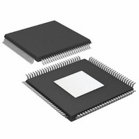
AD9778ABSVZ Analog Devices Inc, AD9778ABSVZ Datasheet - Page 20

AD9778ABSVZ
Manufacturer Part Number
AD9778ABSVZ
Description
IC,D/A CONVERTER,DUAL,14-BIT,CMOS,TQFP,100PIN
Manufacturer
Analog Devices Inc
Specifications of AD9778ABSVZ
Number Of Bits
14
Data Interface
Parallel
Number Of Converters
2
Voltage Supply Source
Analog and Digital
Power Dissipation (max)
300mW
Operating Temperature
-40°C ~ 85°C
Mounting Type
Surface Mount
Package / Case
100-TQFP Exposed Pad, 100-eTQFP, 100-HTQFP, 100-VQFP
Package
100TQFP EP
Resolution
14 Bit
Conversion Rate
1 GSPS
Architecture
Interpolation Filter
Digital Interface Type
Parallel
Number Of Outputs Per Chip
2
Output Type
Current
Full Scale Error
±2(Typ) %FSR
Integral Nonlinearity Error
±1.5(Typ) LSB
Lead Free Status / RoHS Status
Lead free / RoHS Compliant
For Use With
AD9778A-EBZ - BOARD EVALUATION AD9778A
Settling Time
-
Lead Free Status / RoHS Status
Lead free / RoHS Compliant
Available stocks
Company
Part Number
Manufacturer
Quantity
Price
Company:
Part Number:
AD9778ABSVZ
Manufacturer:
Analog Devices Inc
Quantity:
135
Company:
Part Number:
AD9778ABSVZ
Manufacturer:
Analog Devices Inc
Quantity:
10 000
Part Number:
AD9778ABSVZ
Manufacturer:
ADI/亚德诺
Quantity:
20 000
Company:
Part Number:
AD9778ABSVZRL
Manufacturer:
Analog Devices Inc
Quantity:
10 000
AD9776A/AD9778A/AD9779A
REF –25.28dBm
*AVG
log
10dB
PAVG
10
W1 S2
CENTER 143.88MHz
*RES BW 30kHz
RMS RESULTS
CARRIER POWER
–12.49dBm/
3.84000MHz
–150
–154
–158
–162
–166
–170
f
DAC
–55
–60
–65
–70
–75
–80
–85
–90
Figure 31. AD9779A ACLR for First Adjacent Band W-CDMA,
4× Interpolation, f
Over Output Frequency with a Single-Tone Input at −6 dBFS
0
0
On-Chip Modulation Translates Baseband Signal to IF
Figure 30. AD9779A Noise Spectral Density vs. f
20
40
4× Interpolation, f
FREQ OFFSET
5.000MHz
10.00MHz
15.00MHz
Figure 32. AD9779A W-CDMA Signal,
f
DAC
20
60
= 200MSPS
0dBFS, PLL ENABLED
*ATTEN 4dB
80
DATA
VBW 300kHz
100
REF BW
3.840MHz
3.840MHz
3.840MHz
= 122.88 MSPS, f
40
f
f
OUT
OUT
120
DATA
–6dBFS, PLL DISABLED
(MHz)
(MHz)
f
140
DAC
dBc
–76.75
–80.94
–79.95
= 122.88 MSPS,
0dBFS, PLL DISABLED
LOWER
f
60
DAC
= 800MSPS
160
–3dBFS, PLL DISABLED
SWEEP 162.2ms (601 pts)
dBm
–89.23
–93.43
–92.44
= 400MSPS
DAC
180
/4 Modulation
200
dBc
–77.42
–80.47
–78.96
80
UPPER
SPAN 50MHz
220
OUT
dBm
–89.91
–92.96
–91.45
EXT REF
240
,
100
260
Rev. B | Page 20 of 56
REF –30.28dBm
*AVG
log
10dB
PAVG
10
W1 S2
CENTER 151.38MHz
*RES BW 30kHz
TOTAL CARRIER POWER –12.61dBm/15.3600MHz
REF CARRIER POWER –17.87dBm/3.84000MHz
1 –17.87dBm
2 –20.65dBm
3 –18.26dBm
4 –18.23dBm
Figure 33. AD9779A ACLR for Second Adjacent Band W-CDMA,
–55
–60
–65
–70
–75
–80
–85
–90
–55
–60
–65
–70
–75
–80
–85
–90
Figure 34. AD9779A ACLR for Third Adjacent Band W-CDMA,
4× Interpolation, f
0
0
On-Chip Modulation Translates Baseband Signal to IF
On-Chip Modulation Translates Baseband Signal to IF
Figure 35. AD9779A Multicarrier W-CDMA Signal,
20
20
40
40
0dBFS, PLL ENABLED
4× Interpolation, f
4× Interpolation, f
FREQ OFFSET
5.000MHz
10.00MHz
15.00MHz
–3dBFS, PLL DISABLED
–3dBFS, PLL DISABLED
60
60
*ATTEN 4dB
80
80
DAC
VBW 300kHz
100
100
= 122.88 MSPS, f
INTEG BW
3.840MHz
3.840MHz
3.840MHz
f
f
OUT
OUT
120
120
DATA
DATA
(MHz)
(MHz)
140
140
= 122.88 MSPS,
= 122.88 MSPS,
dBc
–67.70
–70.00
–71.65
0dBFS, PLL ENABLED
–6dBFS, PLL DISABLED
–6dBFS, PLL DISABLED
LOWER
160
160
SWEEP 162.2ms (601 pts)
0dBFS, PLL DISABLED
0dBFS, PLL DISABLED
dBm
–85.57
–97.87
–99.52
DAC
180
180
/4 Modulation
200
200
dBc
–67.70
–69.32
–71.00
SPAN 50MHz
UPPER
220
220
EXT REF
dBm
–85.57
–87.19
–88.88
240
240
260
260


