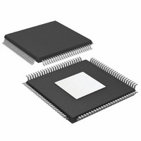
AD9778ABSVZ Analog Devices Inc, AD9778ABSVZ Datasheet - Page 37

AD9778ABSVZ
Manufacturer Part Number
AD9778ABSVZ
Description
IC,D/A CONVERTER,DUAL,14-BIT,CMOS,TQFP,100PIN
Manufacturer
Analog Devices Inc
Specifications of AD9778ABSVZ
Number Of Bits
14
Data Interface
Parallel
Number Of Converters
2
Voltage Supply Source
Analog and Digital
Power Dissipation (max)
300mW
Operating Temperature
-40°C ~ 85°C
Mounting Type
Surface Mount
Package / Case
100-TQFP Exposed Pad, 100-eTQFP, 100-HTQFP, 100-VQFP
Package
100TQFP EP
Resolution
14 Bit
Conversion Rate
1 GSPS
Architecture
Interpolation Filter
Digital Interface Type
Parallel
Number Of Outputs Per Chip
2
Output Type
Current
Full Scale Error
±2(Typ) %FSR
Integral Nonlinearity Error
±1.5(Typ) LSB
Lead Free Status / RoHS Status
Lead free / RoHS Compliant
For Use With
AD9778A-EBZ - BOARD EVALUATION AD9778A
Settling Time
-
Lead Free Status / RoHS Status
Lead free / RoHS Compliant
Available stocks
Company
Part Number
Manufacturer
Quantity
Price
Company:
Part Number:
AD9778ABSVZ
Manufacturer:
Analog Devices Inc
Quantity:
135
Company:
Part Number:
AD9778ABSVZ
Manufacturer:
Analog Devices Inc
Quantity:
10 000
Part Number:
AD9778ABSVZ
Manufacturer:
ADI/亚德诺
Quantity:
20 000
Company:
Part Number:
AD9778ABSVZRL
Manufacturer:
Analog Devices Inc
Quantity:
10 000
INTERPOLATION FILTER BANDWIDTH LIMITS
The AD9776A/AD9778A/AD9779A use a novel interpolation
filter architecture that allows DAC IF frequencies to be gener-
ated anywhere in the spectrum. Figure 68 shows the traditional
choice of DAC IF output bandwidth placement. Note that there
are no possible filter modes in which the carrier can be placed
near 0.5 × f
The filter architecture not only allows the interpolation filter
pass bands to be centered in the middle of the input Nyquist
zones (as explained in this section), but also allows the possi-
bility of a 3 × f
With all of these filter combinations, a carrier of given bandwidth
can be placed anywhere in the spectrum and fall into a possible
pass band of the interpolation filters. The possible bandwidths
accessible with the filter architecture are shown in Figure 69 and
Figure 70. Note that the shifted and nonshifted filter modes are
all accessible by programming the filter mode for a particular
interpolation rate.
Figure 69. Nonshifted Bandwidths Accessible with the Filter Architecture
Figure 68. Traditional Bandwidth Options for TxDAC Output IF
–10
–20
–30
–40
–50
–60
–70
–80
–10
–20
–30
–40
–50
–60
–70
–80
10
10
0
0
–4
–4
DATA
DAC
, 1.5 × f
–3
–3
/8 modulation mode when interpolating by 8.
–2
–2
ASSUMING 8× INTERPOLATION
ASSUMING 8× INTERPOLATION
DATA
f
f
OUT
OUT
, 2.5 × f
–1
–1
(× Input Data Rate),
(× Input Data Rate),
0
0
DATA
, and so on.
1
1
2
2
3
3
4
4
Rev. B | Page 37 of 56
With this filter architecture, a signal placed anywhere in the
spectrum is possible. However, the signal bandwidth is limited
by the input sample rate of the DAC and the specific placement
of the carrier in the spectrum. The bandwidth restriction resulting
from the combination of filter response and input sample rate is
often referred to as the synthesis bandwidth, because this is the
largest bandwidth that the DAC can synthesize.
The maximum bandwidth condition exists if the carrier is
placed directly in the center of one of the filter pass bands. In
this case, the total 0.1 dB bandwidth of the interpolation filters
is equal to 0.8 × f
width as a fraction of the DAC output sample rate drops by a
factor of 2 for every doubling of interpolation rate. The mini-
mum bandwidth condition exists, for example, if a carrier is
placed at 0.25 × f
response is enabled, the high end of the filter response cuts off
at 0.4 × f
If the shifted filter response is instead enabled, then the low end
of the filter response cuts off at 0.1 × f
end of the signal bandwidth. The minimum bandwidth speci-
fication that applies for a carrier at 0.25 × f
f
spectrum for carriers placed at (±n ± 0.25) × f
any integer.
Digital Modulation
The digital quadrature modulation occurs within the interpolation
filter. The modulation shifts the frequency spectrum of the
incoming data by the frequency offset selected. The frequency
offsets available are multiples of the input data rate. The
modulation is equivalent to multiplying the quadrature input
signal by a complex carrier signal, C(t), of the following form:
DATA
Figure 70. Shifted Bandwidths Accessible with the Filter Architecture
. The minimum bandwidth behavior is repeated over the
C(t) = cos(ω
–10
–20
–30
–40
–50
–60
–70
–80
10
DATA
0
–4
, thus limiting the high end of the signal bandwidth.
–3
DATA
DATA
c
t) + j sin(ω
AD9776A/AD9778A/AD9779A
. As Table 19 shows, the synthesis band-
. In this situation, if the nonshifted filter
–2
ASSUMING 8× INTERPOLATION
f
OUT
–1
c
(× Input Data Rate),
t)
0
DATA
1
, thus limiting the low
DATA
2
DATA
is therefore 0.3 ×
, where n is
3
4


