AD9778ABSVZ Analog Devices Inc, AD9778ABSVZ Datasheet - Page 7
AD9778ABSVZ
Manufacturer Part Number
AD9778ABSVZ
Description
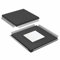
IC,D/A CONVERTER,DUAL,14-BIT,CMOS,TQFP,100PIN
Manufacturer
Analog Devices Inc
Specifications of AD9778ABSVZ
Number Of Bits
14
Data Interface
Parallel
Number Of Converters
2
Voltage Supply Source
Analog and Digital
Power Dissipation (max)
300mW
Operating Temperature
-40°C ~ 85°C
Mounting Type
Surface Mount
Package / Case
100-TQFP Exposed Pad, 100-eTQFP, 100-HTQFP, 100-VQFP
Package
100TQFP EP
Resolution
14 Bit
Conversion Rate
1 GSPS
Architecture
Interpolation Filter
Digital Interface Type
Parallel
Number Of Outputs Per Chip
2
Output Type
Current
Full Scale Error
±2(Typ) %FSR
Integral Nonlinearity Error
±1.5(Typ) LSB
Lead Free Status / RoHS Status
Lead free / RoHS Compliant
For Use With
AD9778A-EBZ - BOARD EVALUATION AD9778A
Settling Time
-
Lead Free Status / RoHS Status
Lead free / RoHS Compliant
Available stocks
Company
Part Number
Manufacturer
Quantity
Price
Company:

Part Number:
AD9778ABSVZ
Manufacturer:
Analog Devices Inc
Quantity:
135
Company:
Part Number:
AD9778ABSVZ
Manufacturer:
Analog Devices Inc
Quantity:
10 000
Part Number:
AD9778ABSVZ
Manufacturer:
ADI/亚德诺
Quantity:
20 000
Company:
Part Number:
AD9778ABSVZRL
Manufacturer:
Analog Devices Inc
Quantity:
10 000


DIGITAL INPUT DATA TIMING SPECIFICATIONS
All modes, −40°C to +85°C.
Table 3.
Parameter
INPUT DATA
LATENCY
3-WIRE INTERFACE
POWER-UP TIME
RESET
1
2
Specified values are with PLL disabled. Timing vs. temperature and data valid keep out windows (that is, the minimum amount of time valid data must be presented to
the device to ensure proper sampling) are delineated in Table 28.
Measured from CSB rising edge when Register 0x00, Bit 4, is written from 1 to 0 with the VREF decoupling capacitor equal to 0.1 μF.
Setup Time
Hold Time
Setup Time
Hold Time
1× Interpolation
2× Interpolation
4× Interpolation
8× Interpolation
Inverse Sync
Maximum Clock Rate (SCLK)
Minimum Pulse Width High, t
Minimum Pulse Width Low, t
Setup Time, t
Hold Time, t
Setup Time, t
Data Valid, t
Minimum Pulse Width, High
1
DV
DH
DS
DS
2
PWL
PWH
Conditions
Input data to DATACLK
Input data to DATACLK
Input data to REFCLK
Input data to REFCLK
With or without modulation
With or without modulation
With or without modulation
With or without modulation
SDIO to SCLK
SDIO to SCLK
CSB to SCLK
SDO to SCLK
Rev. B | Page 7 of 56
Min
3.0
−0.80
−0.05
3.80
2.8
0.0
2.8
2.0
40
Typ
146
297
260
25
70
18
AD9776A/AD9778A/AD9779A
Max
2
12.5
12.5
Unit
ns
ns
ns
ns
DACCLK cycles
DACCLK cycles
DACCLK cycles
DACCLK cycles
DACCLK cycles
MHz
ns
ns
ns
ns
ns
ns
ms
DACCLK cycles
Related parts for AD9778ABSVZ
Image
Part Number
Description
Manufacturer
Datasheet
Request
R

Part Number:
Description:
Dual 16B, 1.0 GSPS TxDAC
Manufacturer:
Analog Devices Inc
Datasheet:
Part Number:
Description:
BOARD EVALUATION FOR AD9778
Manufacturer:
Analog Devices Inc
Datasheet:

Part Number:
Description:
±1.7g Dual-Axis IMEMS Accelerometer Evaluation Board
Manufacturer:
Analog Devices Inc
Datasheet:
Part Number:
Description:
Inertial Sensor Evaluation System
Manufacturer:
Analog Devices Inc
Datasheet:
Part Number:
Description:
Manufacturer:
Analog Devices Inc
Datasheet:
Part Number:
Description:
Manufacturer:
Analog Devices Inc
Datasheet:
Part Number:
Description:
Manufacturer:
Analog Devices Inc
Datasheet:
Part Number:
Description:
Manufacturer:
Analog Devices Inc
Datasheet:
Part Number:
Description:
Manufacturer:
Analog Devices Inc
Datasheet:
Part Number:
Description:
Manufacturer:
Analog Devices Inc
Datasheet:
Part Number:
Description:
Manufacturer:
Analog Devices Inc
Datasheet:
Part Number:
Description:
Manufacturer:
Analog Devices Inc
Datasheet: