ADCMP561BRQZ Analog Devices Inc, ADCMP561BRQZ Datasheet
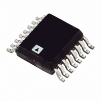
Dual High Speed PECL Comparator

ADCMP561BRQZ

Manufacturer Part Number
ADCMP561BRQZ
Description
Dual High Speed PECL Comparator
Manufacturer
Analog Devices Inc
Type
with Latchr
Datasheet

Specifications of ADCMP561BRQZ

Number Of Elements
2
Output Type
Complementary, Differential, Open-Emitter, PECL
Voltage - Supply
±4.75 V ~ 5.25 V
Mounting Type
Surface Mount
Package / Case
16-LSSOP (0.154", 3.91mm Width)
Number Of Elements
2
Input Offset Voltage
10mV
Input Bias Current (typ)
10uA
Response Time
700ns
Single Supply Voltage (typ)
Not RequiredV
Dual Supply Voltage (typ)
-5.2/5V
Supply Current (max)
13/28@±5VmA
Power Supply Requirement
Dual
Common Mode Rejection Ratio
80dB
Voltage Gain In Db
63dB
Power Supply Rejection Ratio
85dB
Single Supply Voltage (min)
Not RequiredV
Single Supply Voltage (max)
Not RequiredV
Dual Supply Voltage (min)
-4.96/4.75V
Dual Supply Voltage (max)
-5.45/5.25V
Power Dissipation
250mW
Operating Temp Range
-40C to 85C
Operating Temperature Classification
Industrial
Mounting
Surface Mount
Pin Count
16
Package Type
QSOP
No. Of Comparators
2
Ic Output Type
Differential
Output Compatibility
PECL
Supply Current
3.2mA
Supply Voltage Range
4.75V To 5.25V
Amplifier Case Style
QSOP
No. Of Pins
16
Lead Free Status / RoHS Status
Lead free / RoHS Compliant
For Use With
EVAL-ADCMP561BRQZ - BOARD EVALUATION ADCMP561BRQZ
Lead Free Status / Rohs Status
Compliant

Available stocks

Company
Part Number
Manufacturer
Quantity
Price
Part Number:
ADCMP561BRQZ
Manufacturer:
AD
Quantity:
20 000
FEATURES
Differential PECL compatible outputs
700 ps propagation delay input to output
75 ps propagation delay dispersion
Input common-mode range: –2.0 V to +3.0 V
Robust input protection
Differential latch control
Internal latch pull-up resistors
Power supply rejection greater than 85 dB
700 ps minimum pulse width
1.5 GHz equivalent input rise time bandwidth
Typical output rise/fall time of 500 ps
ESD protection > 4kV HBM, >200V MM
Programmable hysteresis
APPLICATIONS
Automatic test equipment
High speed instrumentation
Scope and logic analyzer front ends
Window comparators
High speed line receivers
Threshold detection
Peak detection
High speed triggers
Patient diagnostics
Disk drive read channel detection
Hand-held test instruments
Zero-crossing detectors
Line receivers and signal restoration
Clock drivers
GENERAL DESCRIPTION
The ADCMP561/ADCMP562 are high speed comparators
fabricated on Analog Devices’ proprietary XFCB process. The
devices feature a 700 ps propagation delay with less than 75 ps
overdrive dispersion. Dispersion, a measure of the difference in
propagation delay under differing overdrive conditions, is a
particularly important characteristic of comparators. A separate
programmable hysteresis pin is available on the ADCMP562.
A differential input stage permits consistent propagation delay
with a wide variety of signals in the common-mode range from
−2.0 V to +3.0 V. Outputs are complementary digital signals that
Rev. A
Information furnished by Analog Devices is believed to be accurate and reliable.
However, no responsibility is assumed by Analog Devices for its use, nor for any
infringements of patents or other rights of third parties that may result from its use.
Specifications subject to change without notice. No license is granted by implication
or otherwise under any patent or patent rights of Analog Devices. Trademarks and
registered trademarks are the property of their respective owners.
Dual High Speed PECL Comparators
are fully compatible with PECL 10 K and 10 KH logic families.
The outputs provide sufficient drive current to directly drive
transmission lines terminated in 50 Ω to V
input, which is included, permits tracking, track-and-hold, or
sample-and-hold modes of operation. The latch input pins
contain internal pull-ups that set the latch in tracking mode
when left open.
The ADCMP561/ADCMP562 are specified over the industrial
temperature range (−40°C to +85°C).
One Technology Way, P.O. Box 9106, Norwood, MA 02062-9106, U.S.A.
Tel: 781.329.4700
Fax: 781.326.8703
–INA
+INA
Figure 2. ADCMP561 16-Lead QSOP
LEA
LEA
V
V
QA
QA
DD
EE
1
2
3
4
5
6
7
8
ADCMP561
(Not to Scale)
TOP VIEW
NONINVERTING
FUNCTIONAL BLOCK DIAGRAM
INVERTING
ADCMP561/ADCMP562
LATCH ENABLE
INPUT
INPUT
INPUT
16
15
14
13
12
11
10
© 2004 Analog Devices, Inc. All rights reserved.
9
QB
QB
GND
LEB
LEB
V
–INB
+INB
CC
Figure 1.
ADCMP561/
ADCMP562
HYS*
HYSA
+INA
–INA
Figure 3. ADCMP562 20-Lead QSOP
LEA
LEA
*ADCMP562 ONLY
V
V
V
QA
QA
LATCH ENABLE
INPUT
DD
DD
EE
10
1
2
3
4
5
6
7
8
9
ADCMP562
(Not to Scale)
DD
TOP VIEW
Q OUTPUT
Q OUTPUT
− 2 V. A latch
www.analog.com
20
19
18
17
16
15
14
13
12
11
V
QB
QB
GND
LEB
LEB
V
–INB
+INB
HYSB
DD
CC

Related parts for ADCMP561BRQZ

ADCMP561BRQZ Summary of contents

Page 1

FEATURES Differential PECL compatible outputs 700 ps propagation delay input to output 75 ps propagation delay dispersion Input common-mode range: –2 +3.0 V Robust input protection Differential latch control Internal latch pull-up resistors Power supply rejection greater than ...

Page 2

ADCMP561/ADCMP562 TABLE OF CONTENTS Specifications..................................................................................... 3 Absolute Maximum Ratings............................................................ 5 Thermal Considerations.............................................................. 5 ESD Caution.................................................................................. 5 Pin Configurations and Function Descriptions ........................... 6 Typical Performance Characteristics ............................................. 8 Timing Information ....................................................................... 10 Application Information................................................................ 11 REVISION HISTORY 7/04—Data Sheet Changed ...

Page 3

SPECIFICATIONS −5 +3 Table 1. Electrical Characteristics Parameter DC INPUT CHARACTERISTICS Input Voltage Range Input Differential Voltage Input Offset Voltage Input Offset Voltage Channel Matching Offset ...

Page 4

ADCMP561/ADCMP562 Parameter AC PERFORMANCE (continued) Equivalent Input Rise Time Bandwidth Maximum Toggle Rate Minimum Pulse Width RMS Random Jitter Unit-to-Unit Propagation Delay Skew POWER SUPPLY Positive Supply Current Negative Supply Current Logic Supply Current Logic Supply Current Positive Supply Voltage ...

Page 5

ABSOLUTE MAXIMUM RATINGS Table 2. Parameter Supply Voltages Positive Supply Voltage (V to GND) CC Negative Supply Voltage (V to GND) EE Logic Supply Voltage (V to GND) DD Ground Voltage Differential Input Voltages Input Common-Mode Voltage Differential Input Voltage ...

Page 6

ADCMP561/ADCMP562 PIN CONFIGURATIONS AND FUNCTION DESCRIPTIONS ADCMP561 4 LEA TOP VIEW LEA 5 (Not to Scale –INA 7 +INA 8 Figure 4. ADCMP561 16-Lead QSOP Pin Configuration Table 3. Pin ...

Page 7

Pin No. ADCMP561 ADCMP562 Mnemonic 14 17 GND Function Analog Ground. One of two complementary outputs for Channel logic low if the analog voltage at the noninverting input ...

Page 8

ADCMP561/ADCMP562 TYPICAL PERFORMANCE CHARACTERISTICS –5 +3 3.0 2.5 2.0 1.5 1.0 0.5 0 –0.5 –1.0 –2.5 –1.5 –0.5 0.5 NONINVERTING INPUT VOLTAGE (INVERTING VOLTAGE = 0V) ...

Page 9

TEMPERATURE (°C) Figure 12. Propagation Delay vs. Temperature 140 120 100 0.2 0.4 0.6 0.8 1.0 ...

Page 10

ADCMP561/ADCMP562 TIMING INFORMATION LATCH ENABLE LATCH ENABLE DIFFERENTIAL INPUT VOLTAGE Q OUTPUT Q OUTPUT Figure 18 shows the compare and latch features of the ADCMP561/ADCMP562. Table 4 describes the terms in the diagram. Table 4. Timing Descriptions Symbol Timing t ...

Page 11

APPLICATION INFORMATION The ADCMP561/ADCMP562 comparators are very high speed devices. Consequently, high speed design techniques must be employed to achieve the best performance. The most critical aspect of any ADCMP561/ADCMP562 design is the use of a low impedance ground plane. ...

Page 12

ADCMP561/ADCMP562 Propagation delay dispersion is a specification that is important in critical timing applications such as ATE, bench instruments, and nuclear instrumentation. Overdrive dispersion is defined as the variation in propagation delay as the input overdrive conditions are changed (Figure ...

Page 13

TYPICAL APPLICATION CIRCUITS V IN ADCMP561/ ADCMP562 V REF LATCH V DD ENABLE INPUTS ALL RESISTORS 50Ω Figure 22. High Speed Sampling Circuits +V REF ADCMP561/ ADCMP562 V IN ADCMP561/ ADCMP562 –V REF V LATCH ENABLE INPUTS ALL RESISTORS 50Ω ...

Page 14

ADCMP561/ADCMP562 OUTLINE DIMENSIONS 0.010 0.004 COPLANARITY COPLANARITY ORDERING GUIDE Model Temperature Range ADCMP561BRQ −40°C to +85°C ADCMP562BRQ −40°C to +85°C 0.193 BSC 16 9 0.154 BSC 0.236 1 BSC 8 PIN 1 0.069 0.065 0.053 0.049 0.025 0.012 SEATING BSC ...

Page 15

NOTES Rev Page ADCMP561/ADCMP562 ...

Page 16

ADCMP561/ADCMP562 NOTES © 2004 Analog Devices, Inc. All rights reserved. Trademarks and registered trademarks are the property of their respective owners. D04687–0–7/04(A) Rev Page ...

Related keywords