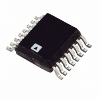
ADCMP561BRQZ Analog Devices Inc, ADCMP561BRQZ Datasheet - Page 3

ADCMP561BRQZ
Manufacturer Part Number
ADCMP561BRQZ
Description
Dual High Speed PECL Comparator
Manufacturer
Analog Devices Inc
Type
with Latchr
Datasheet
1.ADCMP562BRQZ.pdf
(16 pages)
Specifications of ADCMP561BRQZ
Number Of Elements
2
Output Type
Complementary, Differential, Open-Emitter, PECL
Voltage - Supply
±4.75 V ~ 5.25 V
Mounting Type
Surface Mount
Package / Case
16-LSSOP (0.154", 3.91mm Width)
Number Of Elements
2
Input Offset Voltage
10mV
Input Bias Current (typ)
10uA
Response Time
700ns
Single Supply Voltage (typ)
Not RequiredV
Dual Supply Voltage (typ)
-5.2/5V
Supply Current (max)
13/28@±5VmA
Power Supply Requirement
Dual
Common Mode Rejection Ratio
80dB
Voltage Gain In Db
63dB
Power Supply Rejection Ratio
85dB
Single Supply Voltage (min)
Not RequiredV
Single Supply Voltage (max)
Not RequiredV
Dual Supply Voltage (min)
-4.96/4.75V
Dual Supply Voltage (max)
-5.45/5.25V
Power Dissipation
250mW
Operating Temp Range
-40C to 85C
Operating Temperature Classification
Industrial
Mounting
Surface Mount
Pin Count
16
Package Type
QSOP
No. Of Comparators
2
Ic Output Type
Differential
Output Compatibility
PECL
Supply Current
3.2mA
Supply Voltage Range
4.75V To 5.25V
Amplifier Case Style
QSOP
No. Of Pins
16
Lead Free Status / RoHS Status
Lead free / RoHS Compliant
For Use With
EVAL-ADCMP561BRQZ - BOARD EVALUATION ADCMP561BRQZ
Lead Free Status / Rohs Status
Compliant
Available stocks
Company
Part Number
Manufacturer
Quantity
Price
Part Number:
ADCMP561BRQZ
Manufacturer:
AD
Quantity:
20 000
SPECIFICATIONS
V
Table 1. Electrical Characteristics
Parameter
DC INPUT CHARACTERISTICS
LATCH ENABLE CHARACTERISTICS
DC OUTPUT CHARACTERISTICS
AC PERFORMANCE
CC
Input Voltage Range
Input Differential Voltage
Input Offset Voltage
Input Offset Voltage Channel Matching
Offset Voltage Tempco
Input Bias Current
Input Bias Current Tempco
Input Offset Current
Input Capacitance
Input Resistance, Differential Mode
Input Resistance, Common Mode
Active Gain
Common-Mode Rejection Ratio
Hysteresis
Latch Enable Voltage Range
Latch Enable Differential Voltage Range
Latch Enable Input High Current
Latch Enable Input Low Current
LE Voltage, Open
LE Voltage, Open
Latch Setup Time
Latch Hold Time
Latch-to-Output Delay
Latch Minimum Pulse Width
Output Voltage—High Level
Output Voltage—Low Level
Rise Time
Fall Time
Propagation Delay
Propagation Delay Tempco
Prop Delay Skew—Rising Transition to
Within Device Propagation Delay Skew—
Overdrive Dispersion
Overdrive Dispersion
Slew Rate Dispersion
Pulse Width Dispersion
Duty Cycle Dispersion
Common-Mode Voltage Dispersion
= +5.0 V, V
Falling Transition
Channel-to-Channel
EE
= −5.2 V, V
DD
= +3.3 V, T
A
= −40°C to +85°C. Typical values are at T
A
t
t
V
t
Symbol
V
∆V
I
C
CMRR
t
t
V
t
t
∆t
IN
S
H
PLOH
PL
R
F
PD
OS
IN
OH
OL
V
PD
OS
, t
/d
/d
PLOL
T
T
Conditions
V
−IN = −2 V, +IN = +3 V
V
R
@ V
@ V
Latch inputs not connected
Latch inputs not connected
V
V
V
V
PECL 50 Ω to V
PECL 50 Ω to V
10% to 90%
10% to 90%
V
V
V
V
V
20 mV ≤ V
100 mV ≤ V
0.4 V/ns ≤ SR ≤ 1.33 V/ns
700 ps ≤ PW ≤ 10 ns
33 MHz, 1 V/ns, 0.5 V
1 V swing, −1.5 V ≤ V
Rev. A | Page 3 of 16
CM
CM
HYS
OD
OD
OD
OD
OD
OD
OD
OD
OD
DD
DD
= 0 V
= −2.0 V to +3.0 V
= 250 mV
= 250 mV
= 250 mV
= 250 mV
= 1 V
= 20 mV
= 1 V
= 1 V
= 1 V
= ∞
−2.0 V
OD
OD
≤ 100 mV
≤ 1.5 V
DD
DD
− 2.0 V
− 2.0 V
CM
≤ +2.5 V
A
= +25°C, unless otherwise noted.
Min
−2.0
−5
−10.0
−10.0
V
0.4
−300
−300
V
V
V
V
DD
DD
DD
DD
DD
/2 − 0.2
− 2.0
− 0.2
− 1.15
− 1.95
ADCMP561/ADCMP562
Typ
±2.0
±2.0
2.0
±3
0.5
±1.0
0.75
750
1800
63
80
±1.0
V
V
250
250
600
500
550
470
700
830
0.25
50
50
75
75
50
25
15
10
DD
DD
/2
Max
3.0
+5
+10.0
+10.0
V
2.0
+300
+300
V
V
V
V
DD
DD
DD
DD
DD
/2 + 0.2
+ 0.1
− 0.81
− 1.54
Unit
V
V
mV
mV
µV/°C
µA
nA/°C
µA
pF
kΩ
kΩ
dB
dB
mV
V
V
µA
µA
V
V
ps
ps
ps
ps
V
V
ps
ps
ps
ps
ps/°C
ps
ps
ps
ps
ps
ps
ps
ps


