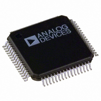
ADE7569ASTZF16-RL Analog Devices Inc, ADE7569ASTZF16-RL Datasheet - Page 17

ADE7569ASTZF16-RL
Manufacturer Part Number
ADE7569ASTZF16-RL
Description
IC,Power Metering,QFP,64PIN,PLASTIC
Manufacturer
Analog Devices Inc
Specifications of ADE7569ASTZF16-RL
Applications
Energy Measurement
Core Processor
8052
Program Memory Type
FLASH (16 kB)
Controller Series
ADE75xx
Ram Size
512 x 8
Interface
I²C, SPI, UART
Number Of I /o
20
Voltage - Supply
3.135 V ~ 3.465 V
Operating Temperature
-40°C ~ 85°C
Mounting Type
Surface Mount
Package / Case
64-LQFP
Lead Free Status / RoHS Status
Lead free / RoHS Compliant
Available stocks
Company
Part Number
Manufacturer
Quantity
Price
Company:
Part Number:
ADE7569ASTZF16-RL
Manufacturer:
Analog Devices Inc
Quantity:
10 000
Preliminary Technical Data
PIN CONFIGURATION AND FUNCTION DESCRIPTIONS
Table 11. Pin Function Descriptions
Pin No.
1
2
3
4
5
6
7
8
9
10
11
12
13
14
15
16
17, 18
19
35 to 20
36
37
38
39
40
41
42
Mnemonic
COM3/FP27
COM2/FP28
COM1
COM0
P1.2/FP25
P1.3/T2EX/FP24
P1.4/T2/FP23
P1.5/FP22
P1.6/FP21
P1.7/FP20
P0.1/FP19
P2.0/FP18
P2.1/FP17
P2.2/FP16
LCDVC
LCDVP2
LCDVB, LCDVA
LCDVP1
FP0 to F15
P1.1/TxD
P1.0/RxD
P0.7/SS/T1
P0.6/SCLK/T0
P0.5/MISO
P0.4/MOSI/SDATA
P0.3/CF2
P1.3/T2EX/FP24
Description
Common Output. COM3 is used for LCD backplane. / LCD Segment Output 27.
Common Output. COM2 is used for LCD backplane. / LCD Segment Output 28.
Common Output. COM1 is used for LCD backplanes.
Common Output. COM0 is used for LCD backplanes.
General-Purpose Digital I/O Port 1.2. / LCD Segment Output 25.
General-Purpose Digital I/O Port 1.3. / Timer 2 Control Input. / LCD Segment Output 24.
General-Purpose Digital I/O Port 1.4. / Timer 2 Input. / LCD Segment Output 23.
General-Purpose Digital I/O Port 1.5. / LCD Segment Output 22.
General-Purpose Digital I/O Port 1.6. / LCD Segment Output 21.
General-Purpose Digital I/O Port 1.7. / LCD Segment Output 20.
General-Purpose Digital I/O Port 0.1. / LCD Segment Output 19.
General-Purpose Digital I/O Port 2.0. / LCD Segment Output 18.
General-Purpose Digital I/O Port 2.1. / LCD Segment Output 17.
General-Purpose Digital I/O Port 2.2. / LCD Segment Output 16.
Output Port for LCD Levels. This pin should be decoupled with a 470 nF capacitor.
Output Port for LCD Levels. These pins should be decoupled with a 470 nF capacitor.
General-Purpose Digital I/O Port 1.1. / Transmitter Data Output 1 (Asynchronous).
General-Purpose Digital I/O Port 1.0. / Receiver Data Input 1 (Asynchronous).
General-Purpose Digital I/O Port 0.6. / Clock Output for I
General-Purpose Digital I/O Port 0.5. / Data in for SPI Port.
General-Purpose Digital I/O Port 0.4. / Data Line I
Analog Output. A 100 nF capacitor should be connected between this pin and LCDVP1 for the internal LCD
charge pump device.
Analog Output. A 100 nF capacitor should be connected between this pin and LCDVP2 for the internal LCD
charge pump device.
LCD Segment Output 0 to LCD Segment Output 15.
General-Purpose Digital I/O Port 0.7. / Slave Select when SPI is in Slave Mode. / Timer 1 Input.
General-Purpose Digital I/O Port 0.3. / Calibration Frequency Logic Output. The CF2 logic output gives
instantaneous active, reactive, or apparent power information.
P1.4/T2/FP23
COM3/FP27
COM2/FP28
P1.2/FP25
P1.5/FP22
P1.6/FP21
P1.7/FP20
P0.1/FP19
P2.0/FP18
P2.1/FP17
P2.2/FP16
LCDVP2
LCDVC
COM1
COM0
10
11
12
13
14
15
16
1
2
3
4
5
6
7
8
9
64 63 62 61 60 59 58 57 56 55 54 53 52 51 50 49
17 18 19 20 21 22 23 24 25 26 27 28 29 30 31 32
PIN 1
ADE7566/ADE7569
Figure 9. Pin Configuration
Rev. PrA | Page 17 of 136
(Not to Scale)
TOP VIEW
2
C-Compatible. / Data Out for SPI Port.
2
C or SPI Port. / Timer 0 Input.
47
46
45
44
43
42
41
40
39
38
37
36
35
34
33
48
INT0
XTAL1
XTAL2
BCTRL/INT1/P0.0
SDEN/P2.3
P0.2/CF1/RTCCAL
P0.3/CF2
P0.4/MOSI/SDATA
P0.5/MISO
P0.6/SCLK/T0
P0.7/SS/T1
P1.0/RxD
P1.1/TxD
FP0
FP1
FP2
ADE7566/ADE7569


