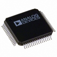
ADE7569ASTZF16-RL Analog Devices Inc, ADE7569ASTZF16-RL Datasheet - Page 48

ADE7569ASTZF16-RL
Manufacturer Part Number
ADE7569ASTZF16-RL
Description
IC,Power Metering,QFP,64PIN,PLASTIC
Manufacturer
Analog Devices Inc
Specifications of ADE7569ASTZF16-RL
Applications
Energy Measurement
Core Processor
8052
Program Memory Type
FLASH (16 kB)
Controller Series
ADE75xx
Ram Size
512 x 8
Interface
I²C, SPI, UART
Number Of I /o
20
Voltage - Supply
3.135 V ~ 3.465 V
Operating Temperature
-40°C ~ 85°C
Mounting Type
Surface Mount
Package / Case
64-LQFP
Lead Free Status / RoHS Status
Lead free / RoHS Compliant
Available stocks
Company
Part Number
Manufacturer
Quantity
Price
Company:
Part Number:
ADE7569ASTZF16-RL
Manufacturer:
Analog Devices Inc
Quantity:
10 000
ADE7566/ADE7569
PHASE COMPENSATION
The ADE7566/ADE7569 must work with transducers that can
have inherent phase errors. For example, a phase error of 0.1° to
0.3° is not uncommon for a current transformer (CT). These
phase errors can vary from part to part, and they must be
corrected to perform accurate power calculations. The errors
associated with phase mismatch are particularly noticeable at
low power factors. The ADE7566/ADE7569 provide a means of
digitally calibrating these small phase errors. The part allows a
small time delay or time advance to be introduced into the
signal processing chain to compensate for small phase errors.
Because the compensation is in time, this technique should only
be used for small phase errors in the range of 0.1° to 0.5°.
Correcting large phase errors using a time shift technique can
introduce significant phase errors at higher harmonics.
The phase calibration register (PHCAL[7:0]) is a twos complement,
signed, single-byte register that has values ranging from 0x82
(−126d) to 0x68 (104d).
The PHCAL register is centered at 0x40, meaning that writing
0x40 to the register gives 0 delay. By changing this register, the
time delay in the voltage channel signal path can change from
−231.93 μs to +48.83 μs (MCLK = 4.096 MHz). One LSB is
equivalent to 1.22 μs (MCLK/5) time delay or advance. A line
frequency of 60 Hz gives a phase resolution of 0.026° at the
fundamental (that is, 360° × 1.22 μs × 60 Hz).
Figure 46 illustrates how the phase compensation is used to
remove a 0.1° phase lead in current channel due to the external
transducer. To cancel the lead (0.1°) in current channel, a phase
lead must also be introduced into voltage channel. The resolution
of the phase adjustment allows the introduction of a phase lead
in increments of 0.026°. The phase lead is achieved by introducing
a time advance into voltage channel. A time advance of 4.88 μs
is made by writing −4 (0x3C) to the time delay block, thus
reducing the amount of time delay by 4.88 μs, or equivalently, a
phase lead of approximately 0.1° at a line frequency of 60 Hz
(0x3C represents −4 because the register is centered with 0 at 0x40).
I
V
I
V
I
V
AP
N
P
N
I
PGA1
PGA2
V
60Hz
ADC 2
0.1°
ADC 1
Figure 46. Phase Calibration
1
–231.93µs TO +48.83µs
7
1
DELAY BLOCK
0
1.22µs/LSB
PHCAL[7:0]
0
1
HPF
0
1
1
24
1
0
CHANNEL 2 DELAY
REDUCED BY 4.48µs
(0.1°LEAD AT 60Hz)
0x0B IN PHCAL[7:0]
24
V
60Hz
I
LPF2
Rev. PrA | Page 48 of 136
RMS CALCULATION
The root mean square (rms) value of a continuous signal V(t) is
defined as
For time sampling signals, rms calculation involves squaring the
signal, taking the average, and obtaining the square root. The
ADE7566/ADE7569 implement this method by serially squaring
the input, averaging them, and then taking the root square of
the average. The averaging part of this signal processing is done
by implementing a low-pass filter (LPF3 in Figure 47, Figure 48
Figure 49). This LPF has a −3dB cut-off frequency of 2 Hz when
MCLK = 4.096 MHz.
where V is the rms voltage.
When this signal goes through LPF3, the cos(2ωt) term is attenu-
ated and only the DC term V
The rms signals can be read from the waveform register by
setting the WAVMODE Register (0x0D) and setting the WFSM
bit in the Interrupt Enable Register 3 SFR (MIRQENH, 0xDB).
Like the current and voltage channels waveform sampling
modes, the waveform date is available at sample rates of
27.9 kSPS, 14 kSPS, 7 kSPS, or 3.5 kSPS.
It is important to note that when the current input is larger than
40% of full scale, the I
represent the true processed rms value. The rms value processed
with this level of input is larger than the 24-bit read by the wave-
form register, making the value read truncated on the high end.
V
V
V
rms
( )
2
t
) (
V (t ) = √2 × V sin(ωt )
INPUT
t
=
=
=
V
2
T
1
2
×
×
−
V
T
∫
0
V
Figure 47. RMS Signal Processing
V
sin(
Preliminary Technical Data
2
2
V
rms
cos
(
2
ω
t
(t) = V
)
waveform sample register does not
t
(
dt
)
2
ω
2
t
rms
– V
)
2
2
goes through (see Figure 47).
cos (2ωt)
LPF3
V
2
(t ) = V
2
V
(3)
(4)
(5)


