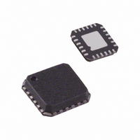
ADF4360-7BCPZRL7 Analog Devices Inc, ADF4360-7BCPZRL7 Datasheet - Page 5

ADF4360-7BCPZRL7
Manufacturer Part Number
ADF4360-7BCPZRL7
Description
IC,FREQUENCY SYNTHESIZER,BICMOS,LLCC,24PIN,PLASTIC
Manufacturer
Analog Devices Inc
Type
Fanout Distribution, Integer N Synthesizer (RF)r
Datasheet
1.ADF4360-7BCPZRL.pdf
(28 pages)
Specifications of ADF4360-7BCPZRL7
Pll
Yes
Input
CMOS
Output
Clock
Number Of Circuits
1
Ratio - Input:output
1:2
Differential - Input:output
No/No
Frequency - Max
1.8GHz
Divider/multiplier
Yes/No
Voltage - Supply
3 V ~ 3.6 V
Operating Temperature
-40°C ~ 85°C
Mounting Type
Surface Mount
Package / Case
24-LFCSP
Frequency-max
1.8GHz
Number Of Elements
1
Pll Input Freq (min)
10MHz
Pll Input Freq (max)
250MHz
Operating Supply Voltage (typ)
3.3V
Operating Temp Range
-40C to 85C
Package Type
LFCSP EP
Output Frequency Range
350 to 1800MHz
Operating Supply Voltage (min)
3V
Operating Supply Voltage (max)
3.6V
Operating Temperature Classification
Industrial
Pin Count
24
Lead Free Status / RoHS Status
Lead free / RoHS Compliant
For Use With
EVAL-ADF4360-7EBZ1 - BOARD EVALUATION FOR ADF4360-7
Lead Free Status / Rohs Status
Compliant
Available stocks
Company
Part Number
Manufacturer
Quantity
Price
Company:
Part Number:
ADF4360-7BCPZRL7
Manufacturer:
AD
Quantity:
3 100
Part Number:
ADF4360-7BCPZRL7
Manufacturer:
ADI/亚德诺
Quantity:
20 000
TIMING CHARACTERISTICS
AV
Table 2.
Parameter
t
t
t
t
t
t
t
1
1
2
3
4
5
6
7
Refer to the
DD
= DV
Power-Up
DD
CLOCK
DATA
= V
LE
LE
VCO
section for the recommended power-up procedure for this device.
= 3.3 V ± 10%; AGND = DGND = 0 V; 1.8 V and 3 V logic levels used; T
Limit at T
20
10
10
25
25
10
20
DB23 (MSB)
t
1
MIN
to T
MAX
t
2
1
(B Version)
DB22
t
3
Figure 2. Timing Diagram
Rev. A | Page 5 of 28
DB2
t
4
t
5
(CONTROL BIT C2)
Unit
ns min
ns min
ns min
ns min
ns min
ns min
ns min
DB1
Test Conditions/Comments
LE Setup Time
DATA to CLOCK Setup Time
DATA to CLOCK Hold Time
CLOCK High Duration
CLOCK Low Duration
CLOCK to LE Setup Time
LE Pulse Width
A
= T
MIN
(CONTROL BIT C1)
to T
DB0 (LSB)
MAX
t
6
, unless otherwise noted.
t
7
ADF4360-7


