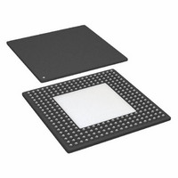
ADSP-21369KBPZ-3A Analog Devices Inc, ADSP-21369KBPZ-3A Datasheet - Page 25

ADSP-21369KBPZ-3A
Manufacturer Part Number
ADSP-21369KBPZ-3A
Description
IC,DSP,32-BIT,CMOS,BGA,256PIN,PLASTIC
Manufacturer
Analog Devices Inc
Series
SHARC®r
Type
Floating Pointr
Datasheet
1.ADSP-21369KBPZ-2A.pdf
(60 pages)
Specifications of ADSP-21369KBPZ-3A
Interface
DAI, DPI
Clock Rate
400MHz
Non-volatile Memory
ROM (768 kB)
On-chip Ram
256kB
Voltage - I/o
3.30V
Voltage - Core
1.20V
Operating Temperature
0°C ~ 70°C
Mounting Type
Surface Mount
Package / Case
256-BGA Exposed Pad, 256-eBGA, 256-HBGA
Lead Free Status / RoHS Status
Lead free / RoHS Compliant
For Use With
ADZS-21369-EZLITE - KIT EVAL EZ LITE ADDS-21369
Lead Free Status / RoHS Status
Lead free / RoHS Compliant
Available stocks
Company
Part Number
Manufacturer
Quantity
Price
Company:
Part Number:
ADSP-21369KBPZ-3A
Manufacturer:
TOREX
Quantity:
6 700
Company:
Part Number:
ADSP-21369KBPZ-3A
Manufacturer:
Analog Devices Inc
Quantity:
10 000
Part Number:
ADSP-21369KBPZ-3A
Manufacturer:
ADI/亚德诺
Quantity:
20 000
Timer WDTH_CAP Timing
The following specification applies to Timer0, Timer1, and
Timer2 in WDTH_CAP (pulse width count and capture) mode.
Timer signals are routed to the DPI_P14–1 pins through the
DPI SRU. Therefore, the specification provided in
valid at the DPI_P14–1 pins.
Table 18. Timer Width Capture Timing
Pin to Pin Direct Routing (DAI and DPI)
For direct pin connections only (for example, DAI_PB01_I to
DAI_PB02_O).
Table 19. DAI/DPI Pin to Pin Routing
Parameter
Switching Characteristic
t
Parameter
Timing Requirement
t
PW
DPIO
I
Timer Pulse Width
Delay DAI/DPI Pin Input Valid to DAI/DPI Output Valid
(TIMER2–0)
DPI_P14–1
DAI_Pm
DPI_Pm
DAI_Pn
DPI_Pn
Figure 14. DAI/DPI Pin to Pin Direct Routing
Figure 13. Timer Width Capture Timing
Table 18
Rev. E | Page 25 of 60 | July 2009
is
Min
2 × t
t
DPIO
PCLK
t
PWI
ADSP-21367/ADSP-21368/ADSP-21369
Min
1.5
Max
2 × (2
31
– 1) × t
PCLK
Max
12
Unit
ns
Unit
ns


