ADSP-21369KBPZ-3A Analog Devices Inc, ADSP-21369KBPZ-3A Datasheet - Page 8
ADSP-21369KBPZ-3A
Manufacturer Part Number
ADSP-21369KBPZ-3A
Description
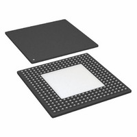
IC,DSP,32-BIT,CMOS,BGA,256PIN,PLASTIC
Manufacturer
Analog Devices Inc
Series
SHARC®r
Type
Floating Pointr
Datasheet
1.ADSP-21369KBPZ-2A.pdf
(60 pages)
Specifications of ADSP-21369KBPZ-3A
Interface
DAI, DPI
Clock Rate
400MHz
Non-volatile Memory
ROM (768 kB)
On-chip Ram
256kB
Voltage - I/o
3.30V
Voltage - Core
1.20V
Operating Temperature
0°C ~ 70°C
Mounting Type
Surface Mount
Package / Case
256-BGA Exposed Pad, 256-eBGA, 256-HBGA
Lead Free Status / RoHS Status
Lead free / RoHS Compliant
For Use With
ADZS-21369-EZLITE - KIT EVAL EZ LITE ADDS-21369
Lead Free Status / RoHS Status
Lead free / RoHS Compliant
Available stocks
Company
Part Number
Manufacturer
Quantity
Price
Company:

Part Number:
ADSP-21369KBPZ-3A
Manufacturer:
TOREX
Quantity:
6 700
Company:
Part Number:
ADSP-21369KBPZ-3A
Manufacturer:
Analog Devices Inc
Quantity:
10 000
Part Number:
ADSP-21369KBPZ-3A
Manufacturer:
ADI/亚德诺
Quantity:
20 000


ADSP-21367/ADSP-21368/ADSP-21369
Asynchronous Memory Controller
The asynchronous memory controller provides a configurable
interface for up to four separate banks of memory or I/O
devices. Each bank can be independently programmed with dif-
ferent timing parameters, enabling connection to a wide variety
of memory devices including SRAM, ROM, flash, and EPROM,
as well as I/O devices that interface with standard memory
control lines. Bank 0 occupies a 14M word window and Banks 1,
2, and 3 occupy a 16M word window in the processor’s address
space but, if not fully populated, these windows are not made
contiguous by the memory controller logic. The banks can also
be configured as 8-bit, 16-bit, or 32-bit wide buses for ease of
interfacing to a range of memories and I/O devices tailored
either to high performance or to low cost and power.
Pulse-Width Modulation
The PWM module is a flexible, programmable, PWM waveform
generator that can be programmed to generate the required
switching patterns for various applications related to motor and
engine control or audio power control. The PWM generator can
generate either center-aligned or edge-aligned PWM wave-
forms. In addition, it can generate complementary signals on
two outputs in paired mode or independent signals in non-
paired mode (applicable to a single group of four PWM
waveforms).
The entire PWM module has four groups of four PWM outputs
each. Therefore, this module generates 16 PWM outputs in
total. Each PWM group produces two pairs of PWM signals on
the four PWM outputs.
The PWM generator is capable of operating in two distinct
modes while generating center-aligned PWM waveforms: single
update mode or double update mode. In single update mode,
the duty cycle values are programmable only once per PWM
period. This results in PWM patterns that are symmetrical
about the midpoint of the PWM period. In double update
mode, a second updating of the PWM registers is implemented
at the midpoint of the PWM period. In this mode, it is possible
to produce asymmetrical PWM patterns that produce lower
harmonic distortion in 2-phase PWM inverters.
Digital Applications Interface (DAI)
The digital applications interface (DAI ) provide the ability to
connect various peripherals to any of the DSP’s DAI pins
(DAI_P20–1). Programs make these connections using the sig-
nal routing unit (SRU1), shown in
The SRU is amatrix routing unit (or group of multiplexers) that
enable the peripherals provided by the DAI to be intercon-
nected under software control. This allows easy use of the
associated peripherals for a much wider variety of applications
by using a larger set of algorithms than is possible with noncon-
figurable signal paths.
The DAI include eight serial ports, an S/PDIF receiver/trans-
mitter, four precision clock generators (PCG), eight channels of
synchronous sample rate converters, and an input data port
(IDP). The IDP provides an additional input path to the
Figure
1.
Rev. E | Page 8 of 60 | July 2009
processor core, configurable as either eight channels of I
data or as seven channels plus a single 20-bit wide synchronous
parallel data acquisition port. Each data channel has its own
DMA channel that is independent from the processor’s serial
ports.
For complete information on using the DAI, see the
ADSP-21368 SHARC Processor Hardware Reference.
Serial Ports
The processors feature eight synchronous serial ports (SPORTs)
that provide an inexpensive interface to a wide variety of digital
and mixed-signal peripheral devices such as Analog Devices’
AD183x family of audio codecs, ADCs, and DACs. The serial
ports are made up of two data lines, a clock, and frame sync. The
data lines can be programmed to either transmit or receive and
each data line has a dedicated DMA channel.
Serial ports are enabled via 16 programmable and simultaneous
receive or transmit pins that support up to 32 transmit or 32
receive channels of audio data when all eight SPORTs are
enabled, or eight full duplex TDM streams of 128 channels
per frame.
The serial ports operate at a maximum data rate of 50 Mbps.
Serial port data can be automatically transferred to and from
on-chip memory via dedicated DMA channels. Each of the
serial ports can work in conjunction with another serial port to
provide TDM support. One SPORT provides two transmit sig-
nals while the other SPORT provides the two receive signals.
The frame sync and clock are shared.
Serial ports operate in five modes:
Left-justified sample pair mode is a mode where in each frame
sync cycle two samples of data are transmitted/received—one
sample on the high segment of the frame sync, the other on the
low segment of the frame sync. Programs have control over var-
ious attributes of this mode.
Each of the serial ports supports the left-justified sample pair
and I
monly used by audio codecs, ADCs, and DACs such as the
Analog Devices AD183x family), with two data pins, allowing
four left-justified sample pair or I
devices) per serial port, with a maximum of up to 32 I
nels. The serial ports permit little-endian or big-endian
transmission formats and word lengths selectable from 3 bits to
32 bits. For the left-justified sample pair and I
word lengths are selectable between 8 bits and 32 bits. Serial
ports offer selectable synchronization and transmit modes as
well as optional -law or A-law companding selection on a per
channel basis. Serial port clocks and frame syncs can be inter-
nally or externally generated.
• Standard DSP serial mode
• Multichannel (TDM) mode with support for packed I
• I
• Packed I
• Left-justified sample pair mode
mode
2
2
S protocols (I
S mode
2
S mode
2
S is an industry-standard interface com-
2
S channels (using two stereo
2
S modes, data-
2
S chan-
2
S serial
2
S
Related parts for ADSP-21369KBPZ-3A
Image
Part Number
Description
Manufacturer
Datasheet
Request
R

Part Number:
Description:
IC DSP 32BIT 266MHZ 208-LQFP
Manufacturer:
Analog Devices Inc
Datasheet:
Part Number:
Description:
IC DSP 32BIT 350MHZ 208-LQFP
Manufacturer:
Analog Devices Inc
Datasheet:

Part Number:
Description:
±1.7g Dual-Axis IMEMS Accelerometer Evaluation Board
Manufacturer:
Analog Devices Inc
Datasheet:

Part Number:
Description:
Inertial Sensor Evaluation System
Manufacturer:
Analog Devices Inc
Datasheet:
Part Number:
Description:
Manufacturer:
Analog Devices Inc
Datasheet:
Part Number:
Description:
Manufacturer:
Analog Devices Inc
Datasheet:
Part Number:
Description:
Manufacturer:
Analog Devices Inc
Datasheet:
Part Number:
Description:
Manufacturer:
Analog Devices Inc
Datasheet:
Part Number:
Description:
Manufacturer:
Analog Devices Inc
Datasheet:
Part Number:
Description:
Manufacturer:
Analog Devices Inc
Datasheet:
Part Number:
Description:
Manufacturer:
Analog Devices Inc
Datasheet:
Part Number:
Description:
Manufacturer:
Analog Devices Inc
Datasheet:
Part Number:
Description:
Manufacturer:
Analog Devices Inc
Datasheet: