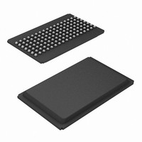
CY7C1355C-133BGCT Cypress Semiconductor Corp, CY7C1355C-133BGCT Datasheet - Page 24

CY7C1355C-133BGCT
Manufacturer Part Number
CY7C1355C-133BGCT
Description
CY7C1355C-133BGCT
Manufacturer
Cypress Semiconductor Corp
Datasheet
1.CY7C1355C-133AXC.pdf
(32 pages)
Specifications of CY7C1355C-133BGCT
Format - Memory
RAM
Memory Type
SRAM - Synchronous
Memory Size
9M (256K x 36)
Speed
133MHz
Interface
Parallel
Voltage - Supply
3.135 V ~ 3.6 V
Operating Temperature
0°C ~ 70°C
Package / Case
119-BGA
Lead Free Status / RoHS Status
Contains lead / RoHS non-compliant
Switching Waveforms
NOP, STALL and DESELECT Cycles
Notes
Document Number: 38-05539 Rev. *H
COMMAND
25. For this waveform ZZ is tied LOW.
26. When CE is LOW, CE
27. The IGNORE CLOCK EDGE or STALL cycle (Clock 3) illustrates CEN being used to create a pause. A write is not performed during this cycle.
ADDRESS
ADV/LD
BW
CEN
CLK
WE
DQ
OE
CE
X
t CENS
t CES
t AS
WRITE
D(A1)
A1
1
1
is LOW, CE
t CENH
t CEH
t AH
t DS
WRITE
D(A1)
D(A2)
A2
2
2
(continued)
t CH
is HIGH and CE
t DH
t CYC
t CL
D(A2+1)
BURST
WRITE
D(A2)
3
[25, 26, 27]
3
is LOW. When CE is HIGH, CE
DON’T CARE
D(A2+1)
READ
Q(A3)
A3
4
t CDV
t CLZ
Q(A4)
READ
Q(A3)
A4
5
t DOH
t OEHZ
1
UNDEFINED
is HIGH or CE
Q(A4+1)
BURST
Q(A4)
READ
6
t OEV
t OELZ
2
is LOW or CE
Q(A4+1)
WRITE
D(A5)
A5
7
t CHZ
t DOH
CY7C1355C, CY7C1357C
3
Q(A6)
READ
is HIGH.
A6
D(A5)
8
WRITE
D(A7)
Q(A6)
A7
9
DESELECT
Page 24 of 32
D(A7)
10
[+] Feedback


