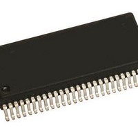
MM908E625ACDWB Freescale Semiconductor, MM908E625ACDWB Datasheet - Page 37

MM908E625ACDWB
Manufacturer Part Number
MM908E625ACDWB
Description
IC QUAD HALF BRDG MCU/LIN 54SOIC
Manufacturer
Freescale Semiconductor
Datasheets
1.MM908E625.pdf
(48 pages)
2.MM908E625ACDWB.pdf
(48 pages)
3.MM908E625ACDWB.pdf
(48 pages)
4.MM908E625ACDWB.pdf
(48 pages)
5.MM908E625ACDWB.pdf
(40 pages)
Specifications of MM908E625ACDWB
Applications
Automotive Mirror Control
Core Processor
HC08
Program Memory Type
FLASH (16 kB)
Controller Series
908E
Ram Size
512 x 8
Interface
SCI, SPI
Number Of I /o
13
Voltage - Supply
8 V ~ 18 V
Operating Temperature
-40°C ~ 85°C
Mounting Type
Surface Mount
Package / Case
54-SOIC (0.300", 7.50mm Width) Exposed Pad
Program Memory Size
16 KB
Number Of Programmable I/os
54
Number Of Timers
16
Operating Supply Voltage
- 18 V to + 28 V
Maximum Operating Temperature
+ 85 C
Mounting Style
SMD/SMT
Minimum Operating Temperature
- 40 C
Lead Free Status / RoHS Status
Contains lead / RoHS non-compliant
Available stocks
Company
Part Number
Manufacturer
Quantity
Price
Company:
Part Number:
MM908E625ACDWB
Manufacturer:
FREESCALE Semiconductor
Quantity:
26
HIGH-SIDE OVERTEMPERATURE PROTECTION
warning with the HTF in the Interrupt Flag Register. In order
to protect the output against overtemperature, the High-
Temperature Reset must be enabled. If this value is reached,
the part generates a reset and disables all power outputs.
HIGH-SIDE OVERCURRENT PROTECTION
the event overcurrent limit is or was reached, the output
automatically switches off and the overcurrent flag is set.
the 908E625 prevents an overcurrent shutdown during this
SWITCHABLE VDD OUTPUT (HVDD)
used for driving external circuitry that requires a V
The output is enabled with bit PSON in the System Control
Register and can be switched on/off with bit HVDDON in the
Power Output Register. Low- or high-voltage conditions (LVI/
HVI) have no influence on this circuitry.
Analog Integrated Circuit Device Data
Freescale Semiconductor
The high-side output provides an overtemperature pre-
The high-side output is protected against overcurrent. In
Due to the high inrush current of bulbs, a special feature of
The HVDD pin is a switchable VDD output pin. It can be
HS Current
FGEN Input
(MCU PWM
Signal)
HS Overcurrent Shutdown Threshold
Figure 22. Inrush Current Limiter on High-Side Output
DD
voltage.
inrush. If an PWM frequency is supplied to the FGEN output
during the switching on of a bulb, the inrush current is limited
to the overcurrent shutdown limit. This means if the current
reaches the overcurrent shutdown, the high side will be
switched off, but each rising edge on the FGEN input will
enable the driver again.
current or a real shutdown, the software must check if the
overcurrent status flag (HS_OCF) in the System Status
Register is set beyond a certain period of time. The
overcurrent status flag is cleared by writing a Logic [1] to the
HS_OCF in the System Status Register, see
HVDD OVERTEMPERATURE PROTECTION
temperature reset is enabled.
HVDD OVERCURRENT PROTECTION
event the overcurrent limit is or was reached, the output
automatically switches off and the HVDD overcurrent flag in
the System Status Register is set.
To distinguish between a shutdown due to an inrush
Overtemperature protection is enabled if the high-
The HVDD output is protected against overcurrent. In the
LOGIC COMMANDS AND REGISTERS
FUNCTIONAL DEVICE OPERATION
Figure
22.
908E625
t
t
37


