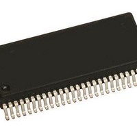
MM908E625ACDWB Freescale Semiconductor, MM908E625ACDWB Datasheet - Page 8

MM908E625ACDWB
Manufacturer Part Number
MM908E625ACDWB
Description
IC QUAD HALF BRDG MCU/LIN 54SOIC
Manufacturer
Freescale Semiconductor
Datasheets
1.MM908E625.pdf
(48 pages)
2.MM908E625ACDWB.pdf
(48 pages)
3.MM908E625ACDWB.pdf
(48 pages)
4.MM908E625ACDWB.pdf
(48 pages)
5.MM908E625ACDWB.pdf
(40 pages)
Specifications of MM908E625ACDWB
Applications
Automotive Mirror Control
Core Processor
HC08
Program Memory Type
FLASH (16 kB)
Controller Series
908E
Ram Size
512 x 8
Interface
SCI, SPI
Number Of I /o
13
Voltage - Supply
8 V ~ 18 V
Operating Temperature
-40°C ~ 85°C
Mounting Type
Surface Mount
Package / Case
54-SOIC (0.300", 7.50mm Width) Exposed Pad
Program Memory Size
16 KB
Number Of Programmable I/os
54
Number Of Timers
16
Operating Supply Voltage
- 18 V to + 28 V
Maximum Operating Temperature
+ 85 C
Mounting Style
SMD/SMT
Minimum Operating Temperature
- 40 C
Lead Free Status / RoHS Status
Contains lead / RoHS non-compliant
Available stocks
Company
Part Number
Manufacturer
Quantity
Price
Company:
Part Number:
MM908E625ACDWB
Manufacturer:
FREESCALE Semiconductor
Quantity:
26
Table 3. Static Electrical Characteristics (continued)
microcontroller chip. Characteristics noted under conditions 9.0 V ≤ V
Typical values noted reflect the approximate parameter mean at T
8
908E625
ELECTRICAL CHARACTERISTICS
STATIC ELECTRICAL CHARACTERISTICS
HIGH-SIDE OUTPUT (HS)
HALF-BRIDGE OUTPUTS (HB1:HB4)
SWITCHABLE V
V
INTERNAL DIE TEMPERATURE SENSOR
HALL-EFFECT SENSOR INPUTS (H1:H3)
LIN Receiver
LIN Wake-Up Threshold
Switch ON Resistance @ T
High-Side Overcurrent Shutdown
Switch ON Resistance @ T
High-Side Overcurrent Shutdown
Low-Side Overcurrent Shutdown
Low-Side Current Limitation @ T
Half-Bridge Output HIGH Threshold for BEMF Detection
Half-Bridge Output LOW Threshold for BEMF Detection
Hysteresis for BEMF Detection
Low-Side Current-to-Voltage Ratio (V
Overcurrent Shutdown Threshold
Voltage Ratio (RATIO
Voltage/Temperature Slope
Output Voltage @ 25°C
Output Voltage
SUP
All characteristics are for the analog chip only. Refer to the 68HC908EY16 specification for characteristics of the
Recessive
Dominant
Threshold
Input Hysteresis
High Side
Low Side
Current Limit 1 (CLS2 = 0, CLS1 = 1, CLS0 = 1)
Current Limit 2 (CLS2 = 1, CLS1 = 0, CLS0 = 0)
Current Limit 3 (CLS2 = 1, CLS1 = 0, CLS0 = 1)
Current Limit 4 (CLS2 = 1, CLS1 = 1, CLS0 = 0)
Current Limit 5 (CLS2 = 1, CLS1 = 1, CLS0 = 1)
CSA = 1
CSA = 0
V
V
SUP
SUP
DOWN-SCALER
< 16.2 V
> 16.2 V
DD
OUTPUT (PH.D.)
VSUP
J
J
= V
Characteristic
= 25
= 25
SUP
J
°
°
= 25
C with I
C with I
/V
ADOUT
ADOUT
°
C
LOAD
LOAD
)
[V]/I
= 1.0 A
= 1.0 A
HB
[A])
A
R
R
= 25°C under nominal conditions unless otherwise noted.
DS(ON)HB_HS
RATIO
DS(ON)HB_LS
R
I
SUP
V
I
HVDDOCT
I
Symbol
V
RATIO
DS(ON)HS
V
RATIO
HBHSOC
V
V
HBLSOC
BEMFHY
I
V
S
BEMFH
HSOC
BEMFL
V
V
V
HALL1
HALL2
I
I
I
I
I
V
V
WTH
CL1
CL2
CL3
CL4
CL5
T
T25
ITH
IHY
IH
IL
to
≤ 16 V, -40°C ≤ T
VSUP
V
H
L
0.01 V
0.6 V
Min
210
300
450
600
0.0
3.9
4.0
2.8
7.0
1.0
4.8
1.7
24
–
–
–
–
–
–
–
–
–
–
–
–
LIN
SUP
Analog Integrated Circuit Device Data
J
≤ 125°C unless otherwise noted.
V
V
V
SUP
SUP
SUP
12.0
Typ
600
425
400
260
370
550
740
-30
-60
2.0
5.1
2.1
55
30
30
19
–
–
–
–
–
–
–
-
/2
/2
1.2
Freescale Semiconductor
0.1 V
0.4 V
V
Max
14.0
5.35
-5.0
700
500
500
315
440
650
880
7.5
7.5
2.5
7.0
3.0
40
15
SUP
–
–
–
0
–
–
–
SUP
LIN
mV/°C
Unit
mΩ
mΩ
V/A
mA
mV
mV
mA
V
V
A
A
A
V
V
V
–


