MT9M001C12STM Aptina LLC, MT9M001C12STM Datasheet
MT9M001C12STM
Specifications of MT9M001C12STM
Q3930625
Q3990821
Available stocks


Related parts for MT9M001C12STM


MT9M001C12STM Summary of contents
Page 1
... Megapixel CMOS Digital Image Sensor MT9M001C12STM (Monochrome) For the latest data sheet, refer to Aptina’s Web site: www.aptina.com Features ® • Aptina DigitalClarity™ CMOS imaging technology • Array Format (5:4): 1,280H x 1,024V (1,310,720 active pixels). Total (incl. dark pixels): 1,312H x 1,048V (1,374,976 pixels) • ...
Page 2
Table of Contents Applications . . . . . . . . . . . . . . . . . . . . . . . . . . . . . . . . . . . . ...
Page 3
List of Tables Table 1: Key Performance Parameters ...
Page 4
List of Figures Figure 1: 48-Pin CLCC Package Pinout Diagram . . . . . . . . . . . . . . . . . . . . . . . . . . . . . . ...
Page 5
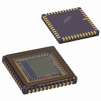
General Description Figure 1: 48-Pin CLCC Package Pinout Diagram STANDBY TRIGGER NC RESET OE GND V A GND A GND PDF:7657919000/Source: 7657919000 MT9M001_DS - Rev. J 5/10 EN MT9M001: 1/2-Inch Megapixel Digital Image Sensor 6 5 ...
Page 6
Figure 2: Block Diagram 1,280H x 1,024V Analog Processing PDF:7657919000/Source: 7657919000 MT9M001_DS - Rev. J 5/10 EN MT9M001: 1/2-Inch Megapixel Digital Image Sensor Control Register Active-Pixel Sensor (APS) Array Timing and Control SXGA ADC 6 General Description Two-wire serial Input/Output ...
Page 7
Table 3: Pin Descriptions Pin Numbers Symbol 29 CLKIN 13 OE# 10 RESET# 46 SCLK 7 STANDBY 8 TRIGGER 45 S DATA 24–28, 32–36 D <0–9> OUT 41 FRAME_VALID 40 LINE_VALID 31 PIXCLK 39 STROBE 15,17,18,21, 47, A GND 48 ...
Page 8
Pixel Data Format Pixel Array Structure The MT9M001 pixel array is configured as 1,312 columns by 1,048 rows (shown in Figure 3). The first 16 columns and the first eight rows of pixels are optically black, and can be used ...
Page 9
Output Data Format The MT9M001 image data is read out in a progressive scan. Valid image data is surrounded by horizontal blanking and vertical blanking, as shown in Figure 5. The amount of horizontal blanking and vertical blanking is programmable ...
Page 10
Figure 7: Row Timing and FRAME_VALID/LINE_VALID Signals FRAME_VALID LINE_VALID Number of master clocks PDF:7657919000/Source: 7657919000 MT9M001_DS - Rev. J 5/10 EN MT9M001: 1/2-Inch Megapixel Digital Image Sensor . . . . . . . . . ...
Page 11
Frame Timing Formulas Table 4: Frame Timing Parameter Name A Active Data Time P Frame Start Blanking 1 P Frame End Blanking Horizontal Blanking Row Time V Vertical Blanking ...
Page 12
Serial Bus Description Registers are written to and read from the MT9M001 through the two-wire serial inter- face bus. The sensor is a two-wire serial interface slave and is controlled by the serial clock (SCLK), which is driven by the ...
Page 13
Stop Bit The stop bit is defined as a LOW-to-HIGH transition of the data line while the clock line is HIGH. Slave Address The 8-bit address of a two-wire serial interface device consists of seven bits of address and 1 ...
Page 14
Two-Wire Serial Interface Sample Write and Read Sequences 16-Bit Write Sequence A typical write sequence for writing 16 bits to a register is shown in Figure 8. A start bit given by the master, followed by the write address, starts ...
Page 15
Feature Description Signal Path The MT9M001 signal path consists of two stages, a programmable gain stage and a programmable analog offset stage. Programmable Gain Stage A total programmable gain available and can be calculated using the following ...
Page 16
Programmable Analog Offset Stage The programmable analog offset stage corrects for analog offset that might be present in the analog signal. The user would need to program register 0x62 appropriately to enable the analog offset correction. The lower eight bits ...
Page 17
Figure 13: Readout of Eight Pixels in Normal and Column Skip Output Mode Normal readout Column skip readout Black Level Calibration The MT9M001 has automatic black level calibration on-chip which can be overridden by the user, as described below and ...
Page 18
Figure 14: Black Level Calibration Flow Chart Pixel Output (signal minus PDF:7657919000/Source: 7657919000 MT9M001_DS - Rev. J 5/10 EN MT9M001: 1/2-Inch Megapixel Digital Image Sensor Gain Selection (color-wise 10-bit ADC reset) Offset Correction Voltage (color-wise) 18 Feature Description ...
Page 19
Still Image Capture with External Synchronization In continuous mode video image capture, the TRIGGER signal should be held LOW or “0.” To capture a still image, the sensor must first be put into snapshot mode by programming a “1” in ...
Page 20
Electrical Specifications Data Output and Propagation Delays By default, the MT9M001 launches pixel data, FRAME_VALID and LINE_VALID with the rising edge of PIXCLK. The expectation is that the user captures D FRAME_VALID and LINE_VALID using the falling edge of PIXCLK. ...
Page 21
Table 7: DC Electrical Characteristics (continued) f (DC Setup Conditions: Symbol Definition I Digital standby current STDBYD /CLK W I Analog standby current STDBYDA . Table 8: AC Electrical Characteristics f (AC Setup Conditions: CLKIN= 48 MHz ...
Page 22
Two-wire Serial Bus Timing The two-wire serial bus operation requires certain minimum master clock cycles between transitions. These are specified in the following diagrams in master clock cycles. Figure 18: Serial Host Interface Start Condition Timing SCLK S DATA Figure ...
Page 23
Figure 22: Acknowledge Signal Timing After an 8-Bit Write to the Sensor SCLK S DATA Figure 23: Acknowledge Signal Timing After an 8-Bit Read from the Sensor SCLK S DATA Note: After a read, the master receiver must pull down ...
Page 24
Quantum Efficiency Figure 24: Quantum Efficiency—Monochrome Image Center Offset and Orientation Figure 25: Image Center Offset 7.75mm Die Center PDF:7657919000/Source: 7657919000 MT9M001_DS - Rev. J 5/10 EN MT9M001: 1/2-Inch Megapixel Digital Image Sensor ...
Page 25
Table 10: Optical Area Dimensions Optical Area SXGA Center of pixel (20, 12) Center of Pixel (1299, 1035) Chip Size, mm (including Seal Ring) Notes and Y coordinates referenced to center of die. 2. Die center = package ...
Page 26
Figure 27: 48-pin CLCC Package Outline Drawing Top View Notes: 1. All exposed metallized area shall be gold plated 60 micro inches min thk. over nickel plated unless otherwise specified in purchase order. 2. Seal area and die attach area ...
Page 27
Revision History Rev ...
Page 28
Page 29, add Figure 17, Data Output Timing Diagram, and Absolute Maximum Ratings, Table 11 • Page 30, update Propagation Delay for Frame_Valid and Line_Valid Signals (Data Output and Propagation Delays • Page 32, delete Quantum Efficiency figure (Color) ...