MT9M001C12STM Aptina LLC, MT9M001C12STM Datasheet - Page 21
MT9M001C12STM
Manufacturer Part Number
MT9M001C12STM
Description
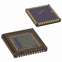
SENSOR IMAGE MONO CMOS 48-LCC
Manufacturer
Aptina LLC
Type
CMOS Imagingr
Datasheets
1.MT9M001C12STM.pdf
(35 pages)
2.MT9M001C12STM.pdf
(2 pages)
3.MT9M001C12STM.pdf
(28 pages)
Specifications of MT9M001C12STM
Pixel Size
5.2µm x 5.2µm
Active Pixel Array
1280H x 1024V
Frames Per Second
30
Voltage - Supply
3 V ~ 3.6 V
Package / Case
48-CLCC
Sensor Image Color Type
Monochrome
Sensor Image Size
1280x1024Pixels
Operating Supply Voltage (min)
3V
Operating Supply Voltage (typ)
3.3V
Operating Supply Voltage (max)
3.6V
Operating Temp Range
0C to 70C
Package Type
CLCC
Operating Temperature Classification
Commercial
Mounting
Surface Mount
Pin Count
48
Lead Free Status / RoHS Status
Lead free / RoHS Compliant
Other names
557-1151
Q3930625
Q3990821
Q3930625
Q3990821
Available stocks
Company
Part Number
Manufacturer
Quantity
Price
Company:

Part Number:
MT9M001C12STM
Manufacturer:
MICRON
Quantity:
1 000
Part Number:
MT9M001C12STM
Manufacturer:
MICRON/镁光
Quantity:
20 000


Table 7:
Table 8:
Table 9:
PDF:7657919000/Source: 7657919000
MT9M001_DS - Rev. J 5/10 EN
Symbol
I
W
I
f
t
T
t
t
t
t
t
t
t
t
t
t
t
t
C
STDBYD
STDBYDA
CLKIIN
CLKIN
R
F
CP
PD
PFH
PLH
PFL
PLL
OS
OH
FVS
LVS
LOAD
/CLK
Symbol
Digital standby current
Analog standby current
Input clock frequency
Input clock period
PIXCLK period
Input clock rise time
Input clock fall time
Clock duty cycle
CLKIN to PIXCLK propagation delay
PIXCLK to data valid
PIXCLK to FV high
PIXCLK to LV high
PIXCLK to FV low
PIXCLK to LV low
Setup time for data before falling edge of PIXCLK
Hold time for data after falling edge of PIXCLK
Setup time for FV before falling edge of PIXCLK
Setup time for LV before falling edge of PIXCLK
Load capacitance
DC Electrical Characteristics (continued)
(DC Setup Conditions:
AC Electrical Characteristics
(AC Setup Conditions:
T
Absolute Maximum Ratings
A
= 25°C))
Definition
Note:
.
Symbol
T
1
only, and functional operation of the device at these or any other conditions above those indicated in
the operational sections of this specification is not implied. Exposure to absolute maximum rating con-
ditions for extended periods may affect reliability.
T
STG 1
f
Stresses greater than those listed may cause permanent damage to the device. This is a stress rating
f
Definition
OP
CLKIN= 48 MHz, V
CLKIN = 48 MHz, V
Operating temperature
Storage temperature
STDBY = V
STDBY = V
DD
DD
= 3.3V, V
= 3.3V, V
DD
DD
Parameter
, CLKIN = 48 MHz
Condition
21
AA
AA
= 3.3V, VAAPIX = 3.3V, Output Load = 30pF,
= 3.3V, VAAPIX = 3.3V, T
MT9M001: 1/2-Inch Megapixel Digital Image Sensor
Condition
T/2 -1
T/2 -1
1000
1000
Min
Min
45
—
—
—
—
—
—
—
—
—
1
2
2
A
Aptina reserves the right to change products or specifications without notice.
= 25°C)
MIN
–40
0
Typ
Rating
55
80
Typ
T/2
T/2
50
10
—
—
—
—
—
—
—
—
4
4
3
3
©2004 Aptina Imaging Corporation. All rights reserved.
Electrical Specifications
MAX
125
70
T/2 +1
T/2 +1
20.83
20.83
Max
Max
48
55
—
13
13
30
—
—
125
100
1
7
7
Unit
MHz
V/ns
V/ns
Unit
Units
°C
°C
ns
ns
ns
ns
ns
ns
ns
ns
pF
ns
ns
ns
ns
%
μA
μA
Related parts for MT9M001C12STM
Image
Part Number
Description
Manufacturer
Datasheet
Request
R

Part Number:
Description:
SENSOR IMAGE VGA COLOR CMOS PLCC
Manufacturer:
Aptina LLC
Datasheet:

Part Number:
Description:
IC SENSOR IMAGE COLOR 48CLCC
Manufacturer:
Aptina LLC
Datasheet:

Part Number:
Description:
SENSOR IMAGE 1.3MP CMOS 48-CLCC
Manufacturer:
Aptina LLC
Datasheet:

Part Number:
Description:
SENSOR IMAGE 2MP CMOS 48-CLCC
Manufacturer:
Aptina LLC
Datasheet:

Part Number:
Description:
SENSOR IMAGE VGA MONO 52IBGA
Manufacturer:
Aptina LLC
Datasheet:

Part Number:
Description:
SENSOR IMAGE VGA COLOR 48CLCC
Manufacturer:
Aptina LLC
Datasheet:

Part Number:
Description:
SENSOR IMAGE COLOR CMOS 48-PLCC
Manufacturer:
Aptina LLC
Datasheet:

Part Number:
Description:
KIT HEAD BOARD FOR MT9P031
Manufacturer:
Aptina LLC
Datasheet:

Part Number:
Description:
KIT HEAD BOARD FOR MT9D131
Manufacturer:
Aptina LLC
Datasheet:

Part Number:
Description:
KIT HEAD BOARD FOR MT9P031
Manufacturer:
Aptina LLC
Datasheet:
Part Number:
Description:
SENSOR IMAGE VGA COLOR CMOS PLCC
Manufacturer:
Aptina LLC
Datasheet:
Part Number:
Description:
IC SENSOR IMAGE COLOR 48CLCC
Manufacturer:
Aptina LLC
Datasheet:
Part Number:
Description:
SENSOR IMAGE 2MP CMOS 48-CLCC
Manufacturer:
Aptina LLC
Datasheet:
