MT9M001C12STM Aptina LLC, MT9M001C12STM Datasheet - Page 9
MT9M001C12STM
Manufacturer Part Number
MT9M001C12STM
Description
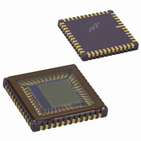
SENSOR IMAGE MONO CMOS 48-LCC
Manufacturer
Aptina LLC
Type
CMOS Imagingr
Datasheets
1.MT9M001C12STM.pdf
(35 pages)
2.MT9M001C12STM.pdf
(2 pages)
3.MT9M001C12STM.pdf
(28 pages)
Specifications of MT9M001C12STM
Pixel Size
5.2µm x 5.2µm
Active Pixel Array
1280H x 1024V
Frames Per Second
30
Voltage - Supply
3 V ~ 3.6 V
Package / Case
48-CLCC
Sensor Image Color Type
Monochrome
Sensor Image Size
1280x1024Pixels
Operating Supply Voltage (min)
3V
Operating Supply Voltage (typ)
3.3V
Operating Supply Voltage (max)
3.6V
Operating Temp Range
0C to 70C
Package Type
CLCC
Operating Temperature Classification
Commercial
Mounting
Surface Mount
Pin Count
48
Lead Free Status / RoHS Status
Lead free / RoHS Compliant
Other names
557-1151
Q3930625
Q3990821
Q3930625
Q3990821
Available stocks
Company
Part Number
Manufacturer
Quantity
Price
Company:

Part Number:
MT9M001C12STM
Manufacturer:
MICRON
Quantity:
1 000
Part Number:
MT9M001C12STM
Manufacturer:
MICRON/镁光
Quantity:
20 000


Output Data Format
Figure 5:
Output Data Timing
Figure 6:
PDF:7657919000/Source: 7657919000
MT9M001_DS - Rev. J 5/10 EN
Spatial Illustration of Image Readout
Timing Example of Pixel Data
The MT9M001 image data is read out in a progressive scan. Valid image data is
surrounded by horizontal blanking and vertical blanking, as shown in Figure 5. The
amount of horizontal blanking and vertical blanking is programmable through Reg0x05
and Reg0x06, respectively. LINE_VALID is HIGH during the shaded region of the figure.
FRAME_VALID timing is described in “Output Data Timing” on page 9.
The data output of the MT9M001 is synchronized with the PIXCLK output. When
LINE_VALID is HIGH, one 10-bit pixel datum is output every PIXCLK period.
The rising edges of the PIXCLK signal are nominally timed to occur on the rising D
edges. This allows PIXCLK to be used as a clock to latch the data. D
the falling edge of PIXCLK. The PIXCLK is HIGH while master clock is HIGH and then
LOW while master clock is LOW. It is continuously enabled, even during the blanking
period. The parameters P1, A, P2, and Q in Figure 7 are defined in Table 4.
D
P
OUT
m-1,0
LINE_VALID
P
P
P
0,0
1,0
00 00 00 ..................................... 00 00 00
00 00 00 ..................................... 00 00 00
00 00 00 ..................................... 00 00 00
00 00 00 ..................................... 00 00 00
m,0
9-D
PIXCLK
P
P
P
0,1
1,1
m-1,1
OUT
P
m,1
P
P
0
0,2
1,2
.....................................P
.....................................P
VERTICAL BLANKING
.....................................P
.....................................P
VALID IMAGE
Blanking
(9:0)
P 0
m-1,n-1
m,n-1
0,n-1
1,n-1
P
m,n
P
P
P
0,n
1,n
m-1,n
(9:0)
P 1
9
00 00 00 .................. 00 00 00
00 00 00 .................. 00 00 00
00 00 00 .................. 00 00 00
00 00 00 .................. 00 00 00
00 00 00 .................. 00 00 00
00 00 00 .................. 00 00 00
00 00 00 .................. 00 00 00
00 00 00 .................. 00 00 00
MT9M001: 1/2-Inch Megapixel Digital Image Sensor
VERTICAL/HORIZONTAL
(9:0)
Valid Image Data
P2
HORIZONTAL
BLANKING
BLANKING
(9:0)
P 3
(9:0)
P 4
. . . .
. . . .
. . . .
. . . .
Aptina reserves the right to change products or specifications without notice.
P n-1
(9:0)
(9:0)
P n
©2004 Aptina Imaging Corporation. All rights reserved.
OUT
Blanking
Pixel Data Format
data is valid on
OUT
Related parts for MT9M001C12STM
Image
Part Number
Description
Manufacturer
Datasheet
Request
R

Part Number:
Description:
SENSOR IMAGE VGA COLOR CMOS PLCC
Manufacturer:
Aptina LLC
Datasheet:

Part Number:
Description:
IC SENSOR IMAGE COLOR 48CLCC
Manufacturer:
Aptina LLC
Datasheet:

Part Number:
Description:
SENSOR IMAGE 1.3MP CMOS 48-CLCC
Manufacturer:
Aptina LLC
Datasheet:

Part Number:
Description:
SENSOR IMAGE 2MP CMOS 48-CLCC
Manufacturer:
Aptina LLC
Datasheet:

Part Number:
Description:
SENSOR IMAGE VGA MONO 52IBGA
Manufacturer:
Aptina LLC
Datasheet:

Part Number:
Description:
SENSOR IMAGE VGA COLOR 48CLCC
Manufacturer:
Aptina LLC
Datasheet:

Part Number:
Description:
SENSOR IMAGE COLOR CMOS 48-PLCC
Manufacturer:
Aptina LLC
Datasheet:

Part Number:
Description:
KIT HEAD BOARD FOR MT9P031
Manufacturer:
Aptina LLC
Datasheet:

Part Number:
Description:
KIT HEAD BOARD FOR MT9D131
Manufacturer:
Aptina LLC
Datasheet:

Part Number:
Description:
KIT HEAD BOARD FOR MT9P031
Manufacturer:
Aptina LLC
Datasheet:
Part Number:
Description:
SENSOR IMAGE VGA COLOR CMOS PLCC
Manufacturer:
Aptina LLC
Datasheet:
Part Number:
Description:
IC SENSOR IMAGE COLOR 48CLCC
Manufacturer:
Aptina LLC
Datasheet:
Part Number:
Description:
SENSOR IMAGE 2MP CMOS 48-CLCC
Manufacturer:
Aptina LLC
Datasheet:
