MT9M001C12STM Aptina LLC, MT9M001C12STM Datasheet - Page 16
MT9M001C12STM
Manufacturer Part Number
MT9M001C12STM
Description
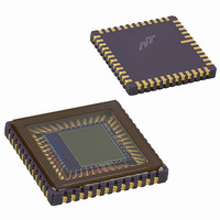
SENSOR IMAGE MONO CMOS 48-LCC
Manufacturer
Aptina LLC
Type
CMOS Imagingr
Datasheets
1.MT9M001C12STM.pdf
(35 pages)
2.MT9M001C12STM.pdf
(2 pages)
3.MT9M001C12STM.pdf
(28 pages)
Specifications of MT9M001C12STM
Pixel Size
5.2µm x 5.2µm
Active Pixel Array
1280H x 1024V
Frames Per Second
30
Voltage - Supply
3 V ~ 3.6 V
Package / Case
48-CLCC
Sensor Image Color Type
Monochrome
Sensor Image Size
1280x1024Pixels
Operating Supply Voltage (min)
3V
Operating Supply Voltage (typ)
3.3V
Operating Supply Voltage (max)
3.6V
Operating Temp Range
0C to 70C
Package Type
CLCC
Operating Temperature Classification
Commercial
Mounting
Surface Mount
Pin Count
48
Lead Free Status / RoHS Status
Lead free / RoHS Compliant
Other names
557-1151
Q3930625
Q3990821
Q3930625
Q3990821
Available stocks
Company
Part Number
Manufacturer
Quantity
Price
Company:

Part Number:
MT9M001C12STM
Manufacturer:
MICRON
Quantity:
1 000
Part Number:
MT9M001C12STM
Manufacturer:
MICRON/镁光
Quantity:
20 000


Programmable Analog Offset Stage
Column and Row Mirror Image
Figure 11:
Figure 12:
Column and Row Skip
PDF:7657919000/Source: 7657919000
MT9M001_DS - Rev. J 5/10 EN
Readout of Six Columns in Normal and Column Mirror Output Mode
Readout of Six Rows in Normal and Row Mirror Output Mode
The programmable analog offset stage corrects for analog offset that might be present in
the analog signal. The user would need to program register 0x62 appropriately to enable
the analog offset correction.
The lower eight bits (bit[7:0]) determines the absolute value of the analog offset to be
corrected and bit[8] determines the sign of the correction. When bit[8] is “1”, the sign of
the correction is negative and vice versa. The analog value of the correction relative to
the analog gain stage can be determined from the following formula:
By setting bit 14 of Reg0x20, the readout order of the columns will be reversed, as shown
in Figure 11.
By setting bits 15 of Reg0x20 the readout order of the rows will be reversed, as shown in
Figure 12.
Normal readout
Reverse readout
By setting bit 3 of Reg0x20, only half of the columns set will be read out. An example is
shown in Figure 13. Only columns with bit 1 equal to “0” will be read out (xxxxxxx0x).
The row skip works in the same way and will only read out rows with bit 1 equal to “0.”
Row skip mode is enabled by setting bit 4 of Reg0x20. For both row and column skips, the
number of rows or columns read out will be half of what is set in Reg0x03 or Reg0x04,
respectively.
Reverse readout
Normal readout
FRAME_VALID
D
D
Analog offset (bit[8] = 0) = bit[7:0] x 2mV
Analog offset (bit[8] = 1) = - (bit[7:0] x 2mV)
OUT
OUT
D
D
LINE_VALID
OUT
OUT
9–D
9–D
9–D
9–D
OUT
OUT
OUT
OUT
0
0
0
0
Row0
Row5
(9:0)
(9:0)
Col0
(9:0)
Col5
(9:0)
Row1
Row4
(9:0)
(9:0)
Col1
(9:0)
Col4
(9:0)
16
MT9M001: 1/2-Inch Megapixel Digital Image Sensor
Row2
Row3
(9:0)
(9:0)
Col2
(9:0)
Col3
(9:0)
Row3
Row2
(9:0)
(9:0)
Col3
(9:0)
Col2
(9:0)
Row4
Row1
(9:0)
(9:0)
(9:0)
(9:0)
Col4
Col1
Aptina reserves the right to change products or specifications without notice.
Row5
Row0
(9:0)
(9:0)
Col5
(9:0)
Col0
(9:0)
©2004 Aptina Imaging Corporation. All rights reserved.
Feature Description
Related parts for MT9M001C12STM
Image
Part Number
Description
Manufacturer
Datasheet
Request
R

Part Number:
Description:
SENSOR IMAGE VGA COLOR CMOS PLCC
Manufacturer:
Aptina LLC
Datasheet:

Part Number:
Description:
IC SENSOR IMAGE COLOR 48CLCC
Manufacturer:
Aptina LLC
Datasheet:

Part Number:
Description:
SENSOR IMAGE 1.3MP CMOS 48-CLCC
Manufacturer:
Aptina LLC
Datasheet:

Part Number:
Description:
SENSOR IMAGE 2MP CMOS 48-CLCC
Manufacturer:
Aptina LLC
Datasheet:

Part Number:
Description:
SENSOR IMAGE VGA MONO 52IBGA
Manufacturer:
Aptina LLC
Datasheet:

Part Number:
Description:
SENSOR IMAGE VGA COLOR 48CLCC
Manufacturer:
Aptina LLC
Datasheet:

Part Number:
Description:
SENSOR IMAGE COLOR CMOS 48-PLCC
Manufacturer:
Aptina LLC
Datasheet:

Part Number:
Description:
KIT HEAD BOARD FOR MT9P031
Manufacturer:
Aptina LLC
Datasheet:

Part Number:
Description:
KIT HEAD BOARD FOR MT9D131
Manufacturer:
Aptina LLC
Datasheet:

Part Number:
Description:
KIT HEAD BOARD FOR MT9P031
Manufacturer:
Aptina LLC
Datasheet:
Part Number:
Description:
SENSOR IMAGE VGA COLOR CMOS PLCC
Manufacturer:
Aptina LLC
Datasheet:
Part Number:
Description:
IC SENSOR IMAGE COLOR 48CLCC
Manufacturer:
Aptina LLC
Datasheet:
Part Number:
Description:
SENSOR IMAGE 2MP CMOS 48-CLCC
Manufacturer:
Aptina LLC
Datasheet:
