CYIL1SM4000AA-GDC Cypress Semiconductor Corp, CYIL1SM4000AA-GDC Datasheet - Page 10
CYIL1SM4000AA-GDC
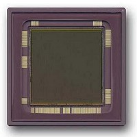
Manufacturer Part Number
CYIL1SM4000AA-GDC
Description
SENSOR IMAGE 4MP CMOS 127-PGA
Manufacturer
Cypress Semiconductor Corp
Type
CMOS Imagingr
Datasheet
1.CYIL1SM4000-EVAL.pdf
(32 pages)
Specifications of CYIL1SM4000AA-GDC
Package / Case
127-PGA
Pixel Size
12µm x 12µm
Active Pixel Array
2048H x 2048V
Frames Per Second
15
Voltage - Supply
2.5V, 3.3V
Operating Supply Voltage
2.5 V
Maximum Operating Temperature
+ 60 C
Minimum Operating Temperature
0 C
Image Size
2048 H x 2048 V
Color Sensing
Monochrome
Package
127CPGA
Operating Temperature
0 to 60 °C
Lead Free Status / RoHS Status
Contains lead / RoHS non-compliant
Lead Free Status / RoHS Status
Lead free / RoHS Compliant, Contains lead / RoHS non-compliant
Other names
LUPA-4000-M
LUPA-4000-M
LUPA-4000-M


Biasing and Analog Signals
The expected analog output levels are between 0.3 V for a white, saturated, pixel and 1.3 V for a black pixel.
There are two output stages, each consisting of two output amplifiers, resulting in four outputs. One output amplifier is used for the
analog signal resulting from the pixels. The second amplifier is used for a DC reference signal. The DC level from the buffer is defined
by a DAC, which is controlled by a 7-bit word downloaded in the SPI. Additionally, an extra bit in the SPI defines if one or two output
stages are used.
Table 3
dissipation, several biasing resistors are required. This optimisation results in an increase of signal swing and dynamic range.
Table 3. Overview of Bias Signals
Each biasing signal determines the operation of a corresponding
module in the sense that it controls speed and dissipation. Some
modules have two biasing resistors: one to achieve the high
speed and another to minimize power dissipation.
Pixel Array Signals
The pixel array of the image sensor requires digital control
signals and several different power supplies. This section
explains the relation between the control signals and the applied
supplies, and the internal generated pixel array signals.
Figure 11
Reset, Sample, Precharge, Vmem, and Row_select. These are
internal generated signals derived by on-chip drivers from
external applied signals. Row_select is generated by the
y-addressing and is not discussed in this section.
Reset: Resets the pixel and initiates the integration time. If reset
is high, then the photodiode is forced to a certain voltage. This
depends on Vpix (pixel supply) and the high level of reset signal.
The higher these signals or supplies, the higher the
voltage-swing. The limitation on the high level of reset and Vpix
is 3.3 V. It does not help to increase Vpix without increasing the
Document Number: 38-05712 Rev. *F
Out_load
dec_x_load
muxbus_load
nsf_load
uni_load_fast
uni_load
pre_load
col_load
dec_y_load
psf_load
precharge_bias
Signal
summarizes the biasing signals required to drive this image sensor. To optimize biasing of column amplifiers to power
illustrates the internal generated pixel array signals:
Connect with 60 KΩ to Voo and capacitor of 100 nF to Gnd
Connect with 2 MΩ to Vdd and capacitor of 100 nF to Gnd
Connect with 25 KΩ to Vaa and capacitor of 100 nF to Gnd
Connect with 5 KΩ to Vaa and capacitor of 100 nF to Gnd
Connect with 10 KΩ to Vaa and capacitor of 100 nF to Gnd
Connect with 1 MΩ to Vaa and capacitor of 100 nF to Gnd
Connect with 3 KΩ to Vaa and capacitor of 100 nF to Gnd
Connect with 1 MΩ to Vaa and capacitor of 100 nF to Gnd
Connect with 2 MΩ to Vdd and capacitor of 100 nF to Gnd
Connect with 1 MΩ to Vaa and capacitor of 100 nF to Gnd
Connect with 1 kΩ to Vdd and capacitor of at least 200 nF to Gnd Pixel drivers
Comment
reset level. The opposite is true. Additionally, it is the reset pulse
that also controls the dual or multiple slope feature inside the
pixel. By giving a reset pulse during integration, but not at full
reset level, the photodiode is reset to a new value, only if this
value is decreased due to light illumination.
The low level of reset is 0 V, but the high level is 2.5 V or higher
(3.3 V) for the normal reset and a lower (<2.5 V) level for the
multiple slope reset.
Precharge: Precharge serves as a load for the first source
follower in the pixel and is activated to overwrite the current
information on the storage node by the new information on the
photodiode. Precharge is controlled by an external digital signal
between 0 V and 2.5 V.
Sample: Samples the photodiode information onto the memory
element. This signal is also a standard digital level between 0 V
and 2.5 V.
Vmem: This signal increases the information on the memory
element with a certain offset. This increases the output voltage
variation. Vmem changes between Vmem_l (2.5 V) and
Vmem_h (3.3 V).
Output stage
X-addressing
Multiplex bus
Column amplifiers
Column amplifiers
Column amplifiers
Column amplifiers
Column amplifiers
Y-addressing
Column amplifiers
Related Module
CYIL1SM4000AA
DC Level
Page 10 of 32
0.7 V
0.4 V
0.8 V
1.2 V
1.2 V
0.5 V
1.4 V
0.5 V
0.4 V
0.5 V
1.4 V
Related parts for CYIL1SM4000AA-GDC
Image
Part Number
Description
Manufacturer
Datasheet
Request
R

Part Number:
Description:
Manufacturer:
Cypress Semiconductor Corp
Datasheet:
Part Number:
Description:
Manufacturer:
Cypress Semiconductor Corp
Datasheet:
Part Number:
Description:
Manufacturer:
Cypress Semiconductor Corp
Datasheet:
Part Number:
Description:
Manufacturer:
Cypress Semiconductor Corp
Datasheet:
Part Number:
Description:
Manufacturer:
Cypress Semiconductor Corp
Datasheet: