CYIL1SM4000AA-GDC Cypress Semiconductor Corp, CYIL1SM4000AA-GDC Datasheet - Page 12
CYIL1SM4000AA-GDC
Manufacturer Part Number
CYIL1SM4000AA-GDC
Description
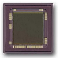
SENSOR IMAGE 4MP CMOS 127-PGA
Manufacturer
Cypress Semiconductor Corp
Type
CMOS Imagingr
Datasheet
1.CYIL1SM4000-EVAL.pdf
(32 pages)
Specifications of CYIL1SM4000AA-GDC
Package / Case
127-PGA
Pixel Size
12µm x 12µm
Active Pixel Array
2048H x 2048V
Frames Per Second
15
Voltage - Supply
2.5V, 3.3V
Operating Supply Voltage
2.5 V
Maximum Operating Temperature
+ 60 C
Minimum Operating Temperature
0 C
Image Size
2048 H x 2048 V
Color Sensing
Monochrome
Package
127CPGA
Operating Temperature
0 to 60 °C
Lead Free Status / RoHS Status
Contains lead / RoHS non-compliant
Lead Free Status / RoHS Status
Lead free / RoHS Compliant, Contains lead / RoHS non-compliant
Other names
LUPA-4000-M
LUPA-4000-M
LUPA-4000-M


■
■
■
■
Test Signals
The test structures implemented in this image sensor are:
■
■
■
Table 5. Frame Rate as Function of ROI Read Out and Sub Sampling
Document Number: 38-05712 Rev. *F
Notes
2048 × 2048
1024 × 2048
1024 × 1024
640 × 480
10. AH: Active High
11. AL: Active Low
Sh_kol (AL
in sample and hold mode and binning mode.
Norowsel (AH
Timing and Readout of Image
Pre_col (AL
row blanking time.
Voltage averaging (AH
averaging of two pixels.
Array of pixels (6 × 12) that outputs are tied together: used for
spectral response measurement.
Temperature diode (2): Apply a forward current of 10 μA to
100 μA and measure the voltage V
linear with the temperature (V
1.6 mV/°C).
End of scan pulses (do not use to trigger other signals):
❐
❐
❐
Image Resolution (X*Y)
Eos_x: end of scan signal: is an output signal, indicating when
the end of line is reached. It is not generated when
windowing.
Eos_y: end of scan signal: is an output signal, indicating when
the end of frame is reached. It is not generated when
windowing.
Eos_spi: output signal of the SPI to check if the data is
transferred correctly through the SPI.
[11]
[11]
): Control signal of the column readout. It is used
[10]
): Control signal of the column readout to reduce
): Control signal of the column readout (see
[10]
): Signal required obtaining voltage
T
Sensor).
decreases with approximately
Frame Rate [frames f/S]
T
of the diode. V
210
15
31
62
T
varies
Frame Readout Time [mS]
Frame Rate and Windowing
Frame Rate
To acquire a frame rate of 15 frames/sec, the output amplifier
should run at 66 MHz pixel rate or two output amplifiers should
run at 33 MHz each, assuming an ROT of 200 ns.
The frame period of the LUPA 4000 sensor is calculated as
follows:
Frame period = FOT + (Nr. Lines × (ROT + pixel period × Nr.
Pixels) with:
FOT = 5 μs
Nr. Lines: Number of Lines read out each frame (Y)
Nr. Pixels: Number of pixels read out each line (X)
ROT = 200 ns (nominal; can be further reduced)
Pixel period: 1/66 MHz = 15.15 ns
Example read out of the full resolution at nominal speed (66 MHz
pixel rate):
Frame period = 5 µs + (2048 × (200 ns + 15.15 ns × 2048)
= 64 ms ≥ 15 fps.
ROI Readout (Windowing)
Windowing is achieved by an SPI in which the starting point of
the x-address and y-address is uploaded. This downloaded
starting point initiates the shift register in the x-direction and
y-direction triggered by the Sync_x and Sync_y pulse. The
minimum step size for the x-address and the y-address is 2 (only
even start addresses can be chosen). The size of both address
registers is 10-bits. For instance, when the addresses
0000000001 and 0000000001 are uploaded, the readout starts
at line 2 and column 2.
4.7
67
32
16
Full resolution.
Subsample in X-direction.
ROI read out.
ROI read out.
CYIL1SM4000AA
Comment
Page 12 of 32
Related parts for CYIL1SM4000AA-GDC
Image
Part Number
Description
Manufacturer
Datasheet
Request
R

Part Number:
Description:
Manufacturer:
Cypress Semiconductor Corp
Datasheet:
Part Number:
Description:
Manufacturer:
Cypress Semiconductor Corp
Datasheet:
Part Number:
Description:
Manufacturer:
Cypress Semiconductor Corp
Datasheet:
Part Number:
Description:
Manufacturer:
Cypress Semiconductor Corp
Datasheet:
Part Number:
Description:
Manufacturer:
Cypress Semiconductor Corp
Datasheet: