CYIL1SM4000AA-GDC Cypress Semiconductor Corp, CYIL1SM4000AA-GDC Datasheet - Page 14
CYIL1SM4000AA-GDC
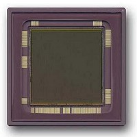
Manufacturer Part Number
CYIL1SM4000AA-GDC
Description
SENSOR IMAGE 4MP CMOS 127-PGA
Manufacturer
Cypress Semiconductor Corp
Type
CMOS Imagingr
Datasheet
1.CYIL1SM4000-EVAL.pdf
(32 pages)
Specifications of CYIL1SM4000AA-GDC
Package / Case
127-PGA
Pixel Size
12µm x 12µm
Active Pixel Array
2048H x 2048V
Frames Per Second
15
Voltage - Supply
2.5V, 3.3V
Operating Supply Voltage
2.5 V
Maximum Operating Temperature
+ 60 C
Minimum Operating Temperature
0 C
Image Size
2048 H x 2048 V
Color Sensing
Monochrome
Package
127CPGA
Operating Temperature
0 to 60 °C
Lead Free Status / RoHS Status
Contains lead / RoHS non-compliant
Lead Free Status / RoHS Status
Lead free / RoHS Compliant, Contains lead / RoHS non-compliant
Other names
LUPA-4000-M
LUPA-4000-M
LUPA-4000-M


Timing specifications for each signal are shown in
■
■
■
■
The timing of the pixel array is straightforward. Before the frame
is read, the information on the photodiode must be stored onto
the memory element inside the pixels. This is done with the
signals Mem_hl, precharge, and sample. When precharge is
activated, it serves as a load for the first source follower in the
pixel. Sample stores the photodiode information onto the
The readout of an image consists of the FOT and the sequential selection of all pixels. The FOT is the overhead time between two
frames to transfer the information on the photodiode to the memory elements.
5 μs). After the FOT, the information is stored into the memory elements and a sequential selection of rows and columns makes sure
the frame is read.
Document Number: 38-05712 Rev. *F
Table 6. Timing Specifications
a
b
c
d
e
Falling edge of precharge is equal or later than falling edge of
Vmem.
Sample is overlapping with precharge.
Rising edge of Vmem is more than 200 ns after rising edge of
sample.
Rising edge of reset is equal or later than rising edge of Vmem.
Symbol
Mem_HL
Precharge
Sample
Precharge-Sample
Integration time
Name
Figure 15. Readout of Image Sensor (L: line selection, C: column selection)
FOT
ROT
Readout frame I
5 - 8.2 μs
3 - 6 μs
5 - 8 μs
> 2 μs
> 1 μs
Value
Table
L1
C1
Readout Lines
Readout Pixels
6.
L2
C2
memory element. Mem_hl pumps up this value to reduce the loss
of signal in the pixel and this signal must be the envelop of
precharge and sample. After Mem_hl is high again, the readout
of the pixel array starts. The frame blanking time or frame
overhead time is thus the time that Mem_hl is low, which is about
5 μs. After the readout starts, the photodiodes can all be
initialised by reset for the next integration time. The minimal
integration time is the minimal time between the falling edge of
reset and the rising edge of sample. Keeping the slow fall times
of the corresponding internal generated signals in mind, the
minimal integration time is about 2 μs.
An additional reset pulse of minimum 2 μs can be given during
integration by asserting Reset_ds to implement the double slope
integration mode.
Readout of Image Sensor
When the pixel information is stored in the memory element of
each pixel, it can be read out sequentially. Integration and
readout can also be done in parallel.
The readout timing is straightforward and is controlled by sync
and clock pulses.
Figure 15
of a frame consists of the frame overhead time, the selection of
the lines sequentially, and the readout of the pixels of the
selected line.
_ _ _
_ _ _
Integration I+2
Figure 14
shows the top level concept of this timing. The readout
shows that at this time Mem_hl is low (typically
C2048
L2048
CYIL1SM4000AA
Page 14 of 32
Related parts for CYIL1SM4000AA-GDC
Image
Part Number
Description
Manufacturer
Datasheet
Request
R

Part Number:
Description:
Manufacturer:
Cypress Semiconductor Corp
Datasheet:
Part Number:
Description:
Manufacturer:
Cypress Semiconductor Corp
Datasheet:
Part Number:
Description:
Manufacturer:
Cypress Semiconductor Corp
Datasheet:
Part Number:
Description:
Manufacturer:
Cypress Semiconductor Corp
Datasheet:
Part Number:
Description:
Manufacturer:
Cypress Semiconductor Corp
Datasheet: