MBRB3030CTLG ON Semiconductor, MBRB3030CTLG Datasheet
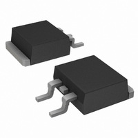
DIODE SCHOTTKY 30V 15A D2PAK

MBRB3030CTLG

Manufacturer Part Number
MBRB3030CTLG
Description
DIODE SCHOTTKY 30V 15A D2PAK
Manufacturer
ON Semiconductor
Series
SWITCHMODE™r
Datasheet

Specifications of MBRB3030CTLG

Voltage - Forward (vf) (max) @ If
440mV @ 15A
Current - Reverse Leakage @ Vr
2mA @ 30V
Current - Average Rectified (io) (per Diode)
15A
Voltage - Dc Reverse (vr) (max)
30V
Diode Type
Schottky
Speed
Fast Recovery =< 500ns, > 200mA (Io)
Diode Configuration
1 Pair Common Cathode
Mounting Type
Surface Mount
Package / Case
D²Pak, TO-263 (2 leads + tab)
Lead Free Status / RoHS Status
Lead free / RoHS Compliant
Reverse Recovery Time (trr)
-

Available stocks

Company
Part Number
Manufacturer
Quantity
Price
Part Number:
MBRB3030CTLG
Manufacturer:
ON
Quantity:
12 500
Part Number:
MBRB3030CTLG
Manufacturer:
ON/安森美
Quantity:
20 000
MBRB3030CTL
SWITCHMODEt
Power Rectifier
with a proprietary barrier metal.
Features
Mechanical Characteristics
Maximum ratings are those values beyond which device damage can occur.
Maximum ratings applied to the device are individual stress limit values (not
normal operating conditions) and are not valid simultaneously. If these limits are
exceeded, device functional operation is not implied, damage may occur and
reliability may be affected.
MAXIMUM RATINGS
© Semiconductor Components Industries, LLC, 2005
August, 2005 − Rev. 6
Peak Repetitive Reverse Voltage
Average Rectified Forward Current
(At Rated V
Peak Repetitive Forward Current
Non−Repetitive Peak Surge Current
Peak Repetitive Reverse Surge Current
Storage Temperature Range
Operating Junction Temperature Range
Voltage Rate of Change
Reverse Energy, Unclamped Inductive
These state−of−the−art devices use the Schottky Barrier principle
Leads are Readily Solderable
260°C Max. for 10 Seconds
Dual Diode Construction, May be Paralleled for Higher Current Output
Guard−Ring for Stress Protection
Low Forward Voltage Drop
125°C Operating Junction Temperature
Maximum Die Size
Short Heat Sink Tab Manufactured − Not Sheared!
Pb−Free Package is Available
Case: Epoxy, Molded, Epoxy Meets UL 94 V−0
Weight: 1.7 Grams (Approximately)
Finish: All External Surfaces Corrosion Resistant and Terminal
Lead and Mounting Surface Temperature for Soldering Purposes:
Device Meets MSL1 Requirements
ESD Ratings: Machine Model, C (>400 V)
Working Peak Reverse Voltage
DC Blocking Voltage
(At Rated V
20 kHz, T
(Surge Applied at Rated Load Conditions
Halfwave, Single Phase, 60 Hz)
(1.0 ms, 1.0 kHz)
(Rated V
Surge (T
J
R
R
C
, T
, T
= 25°C, L = 3.0 mH)
R
= 115°C)
C
J
, Square Wave,
= 25°C)
Rating
= 115°C) Per Device
Human Body Model, 3B (>8000 V)
Symbol
V
V
dV/dt
I
I
I
E
T
FRM
RRM
RWM
FSM
RRM
V
T
I
stg
AS
O
R
J
−55 to +150
−55 to +125
10,000
Value
224.5
300
2.0
30
15
30
30
1
V/ms
Unit
mJ
°C
°C
V
A
A
A
A
MBRB3030CTL
MBRB3030CTLG
Device
30 AMPERES, 30 VOLTS
A
Y
WW
B3030CTL
G
AKA
SCHOTTKY BARRIER
ORDERING INFORMATION
MARKING DIAGRAM
http://onsemi.com
1
RECTIFIER
1
3
CASE 418B
B3030CTLG
PLASTIC
3
AY
= Assembly Location
= Year
= Work Week
= Device Code
= Pb−Free Package
= Diode Polarity
(Pb−Free)
Package
D
D
D
2
AKA
2
2
PAK
Publication Order Number:
PAK
PAK
WW
MBRB3030CTL/D
4
50 Units / Rail
50 Units / Rail
4
Shipping

Related parts for MBRB3030CTLG

MBRB3030CTLG Summary of contents

Page 1

... FRM I 300 A FSM I 2.0 A RRM °C T −55 to +150 stg °C T −55 to +125 J dV/dt 10,000 V/ms E 224 MBRB3030CTL MBRB3030CTLG 1 http://onsemi.com SCHOTTKY BARRIER RECTIFIER 30 AMPERES, 30 VOLTS PAK CASE 418B PLASTIC MARKING DIAGRAM AY WW B3030CTLG AKA A = Assembly Location Y = Year WW = Work Week B3030CTL = Device Code G = Pb− ...

Page 2

THERMAL CHARACTERISTICS (All device data is “Per Leg” except where noted.) Characteristic Thermal Resistance, Junction−to−Ambient (Note 1) Thermal Resistance, Junction−to−Case ELECTRICAL CHARACTERISTICS Maximum Instantaneous Forward Voltage (Note 25° ...

Page 3

SQUARE WAVE 15 Ipk/ Ipk/Io = 5.0 10 Ipk/ 5.0 Ipk/ FREQ = 20 kHz CASE TEMPERATURE (°C) C Figure 5. Current Derating ...

Page 4

... Modeling Reverse Energy Characteristics of Power Rectifiers Prepared by: David Shumate & Larry Walker ON Semiconductor Products Sector ABSTRACT Power semiconductor rectifiers are used in a variety of applications where the reverse energy requirements often vary dramatically based on the operating conditions of the application circuit. A characterization method was devised using the Unclamped Inductive Surge (UIS) test technique ...

Page 5

Suggested Method of Characterization INDUCTOR CURRENT TIME (s) Figure 11. Typical Voltage and Current UIS Waveforms Utilizing the UIS test circuit in Figure 10, devices are tested to failure using inductors ranging in value from 0.01 to 159 mH. The ...

Page 6

Table 1. UIS Test Data Á Á Á Á Á Á Á Á Á Á Á Á Á Á Á Á Á Á ...

Page 7

... SEATING PLANE 0.13 (0.005 VARIABLE CONFIGURATION ZONE VIEW W−W 1 10.66 0.42 *For additional information on our Pb−Free strategy and soldering details, please download the ON Semiconductor Soldering and Mounting Techniques Reference Manual, SOLDERRM/D. MBRB3030CTL PACKAGE DIMENSIONS 2 D PAK CASE 418B−04 ISSUE ...

Page 8

... Fax: 480−829−7709 or 800−344−3867 Toll Free USA/Canada Email: orderlit@onsemi.com MBRB3030CTL N. American Technical Support: 800−282−9855 Toll Free USA/Canada Japan: ON Semiconductor, Japan Customer Focus Center 2−9−1 Kamimeguro, Meguro−ku, Tokyo, Japan 153−0051 Phone: 81−3−5773−3850 http://onsemi.com 8 ON Semiconductor Website: http://onsemi ...

Related keywords