MBRB3030CTLG ON Semiconductor, MBRB3030CTLG Datasheet - Page 6
MBRB3030CTLG
Manufacturer Part Number
MBRB3030CTLG
Description
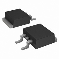
DIODE SCHOTTKY 30V 15A D2PAK
Manufacturer
ON Semiconductor
Series
SWITCHMODE™r
Datasheet
1.MBRB3030CTLG.pdf
(8 pages)
Specifications of MBRB3030CTLG
Voltage - Forward (vf) (max) @ If
440mV @ 15A
Current - Reverse Leakage @ Vr
2mA @ 30V
Current - Average Rectified (io) (per Diode)
15A
Voltage - Dc Reverse (vr) (max)
30V
Diode Type
Schottky
Speed
Fast Recovery =< 500ns, > 200mA (Io)
Diode Configuration
1 Pair Common Cathode
Mounting Type
Surface Mount
Package / Case
D²Pak, TO-263 (2 leads + tab)
Lead Free Status / RoHS Status
Lead free / RoHS Compliant
Reverse Recovery Time (trr)
-
Available stocks
Company
Part Number
Manufacturer
Quantity
Price
Company:

Part Number:
MBRB3030CTLG
Manufacturer:
ON
Quantity:
12 500
Part Number:
MBRB3030CTLG
Manufacturer:
ON/安森美
Quantity:
20 000


Á Á Á Á Á Á Á Á Á Á Á Á Á Á Á Á Á
Á Á Á Á Á Á Á Á Á Á Á Á Á Á Á Á Á
Á Á Á Á
Á Á Á Á
Á Á Á Á
Á Á Á Á
Á Á Á Á
Á Á Á Á
Á Á Á Á
Á Á Á Á
Á Á Á Á
Á Á Á Á
Á Á Á Á
Á Á Á Á
Á Á Á Á
Á Á Á Á
Á Á Á Á
Á Á Á Á
Á Á Á Á
Á Á Á Á
Á Á Á Á
Á Á Á Á
Á Á Á Á
Á Á Á Á
Á Á Á Á
Á Á Á Á
Á Á Á Á
Á Á Á Á
Á Á Á Á
Á Á Á Á
Á Á Á Á
Á Á Á Á
Á Á Á Á
Á Á Á Á
Á Á Á Á
Á Á Á Á
Á Á Á Á
Á Á Á Á
Á Á Á Á
Á Á Á Á
Á Á Á Á
Á Á Á Á
Á Á Á Á
Á Á Á Á
Á Á Á Á
Á Á Á Á
Á Á Á Á
Á Á Á Á
Á Á Á Á
Á Á Á Á
Á Á Á Á
Á Á Á Á
Á Á Á Á
Á Á Á Á
from a reverse energy standpoint, to be used in the
application circuit is as follows:
a. Obtain “Peak Reverse Current versus Time” curve
b. Determine steady state operating voltage (OV) of
c. Determine parasitic inductance (L) of circuit section of
d. Obtain rated breakdown voltage (BVR) of rectifier
e. From the following relationships,
f. The point where the two curves intersect is the current
Table 1. UIS Test Data
1
2
3
4
5
6
7
8
9
10
11
12
13
14
15
16
17
18
19
20
21
22
23
24
25
PART
The procedure to determine if a rectifier is appropriate,
NO.
from data book.
circuit.
interest.
from data book.
a “designer” l versus t curve is plotted alongside the
device characteristic plot.
level where the devices will start to fail. A peak
inductor current below this intersection should be
chosen for safe operating.
V + L @ d
Á Á Á
Á Á Á
Á Á Á
Á Á Á
Á Á Á
Á Á Á
Á Á Á
Á Á Á
Á Á Á
Á Á Á
Á Á Á
Á Á Á
Á Á Á
Á Á Á
Á Á Á
Á Á Á
Á Á Á
Á Á Á
Á Á Á
Á Á Á
Á Á Á
Á Á Á
Á Á Á
Á Á Á
Á Á Á
Á Á Á
Á Á Á
Á Á Á
Á Á Á
Á Á Á
Á Á Á
Á Á Á
Á Á Á
Á Á Á
Á Á Á
Á Á Á
Á Á Á
Á Á Á
Á Á Á
Á Á Á
Á Á Á
Á Á Á
Á Á Á
Á Á Á
Á Á Á
Á Á Á
Á Á Á
Á Á Á
Á Á Á
Á Á Á
Á Á Á
Á Á Á
I
P
46.6
41.7
46.0
42.7
44.9
44.1
26.5
26.4
24.4
27.6
27.7
17.9
18.9
18.8
19.0
74.2
77.3
75.2
77.3
73.8
75.6
74.7
78.4
70.5
78.3
(A)
dt
i(t)
Á Á Á Á
Á Á Á Á
Á Á Á Á
Á Á Á Á
Á Á Á Á
Á Á Á Á
Á Á Á Á
Á Á Á Á
Á Á Á Á
Á Á Á Á
Á Á Á Á
Á Á Á Á
Á Á Á Á
Á Á Á Á
Á Á Á Á
Á Á Á Á
Á Á Á Á
Á Á Á Á
Á Á Á Á
Á Á Á Á
Á Á Á Á
Á Á Á Á
Á Á Á Á
Á Á Á Á
Á Á Á Á
Á Á Á Á
Á Á Á Á
Á Á Á Á
Á Á Á Á
Á Á Á Á
Á Á Á Á
Á Á Á Á
Á Á Á Á
Á Á Á Á
Á Á Á Á
Á Á Á Á
Á Á Á Á
Á Á Á Á
Á Á Á Á
Á Á Á Á
Á Á Á Á
Á Á Á Á
Á Á Á Á
Á Á Á Á
Á Á Á Á
Á Á Á Á
Á Á Á Á
Á Á Á Á
Á Á Á Á
Á Á Á Á
Á Á Á Á
Á Á Á Á
B
VR
65.2
63.4
66.0
64.8
64.8
64.1
63.1
62.8
62.2
62.9
63.2
62.6
62.1
60.7
62.6
69.1
69.6
68.9
69.6
69.1
69.2
68.6
70.3
66.6
69.4
(V)
Á Á Á Á
Á Á Á Á
Á Á Á Á
Á Á Á Á
Á Á Á Á
Á Á Á Á
Á Á Á Á
Á Á Á Á
Á Á Á Á
Á Á Á Á
Á Á Á Á
Á Á Á Á
Á Á Á Á
Á Á Á Á
Á Á Á Á
Á Á Á Á
Á Á Á Á
Á Á Á Á
Á Á Á Á
Á Á Á Á
Á Á Á Á
Á Á Á Á
Á Á Á Á
Á Á Á Á
Á Á Á Á
Á Á Á Á
Á Á Á Á
Á Á Á Á
Á Á Á Á
Á Á Á Á
Á Á Á Á
Á Á Á Á
Á Á Á Á
Á Á Á Á
Á Á Á Á
Á Á Á Á
Á Á Á Á
Á Á Á Á
Á Á Á Á
Á Á Á Á
Á Á Á Á
Á Á Á Á
Á Á Á Á
Á Á Á Á
Á Á Á Á
Á Á Á Á
Á Á Á Á
Á Á Á Á
Á Á Á Á
Á Á Á Á
Á Á Á Á
Á Á Á Á
ENERGY
I +
1038.9
1022.6
1024.9
1091.0
1102.4
1428.6
1547.4
1521.1
1566.2
998.3
870.2
904.2
997.3
865.0
872.0
768.4
815.4
791.7
842.6
752.4
823.2
747.5
834.0
678.4
817.3
(mJ)
(BVR * OV) @ t
Á Á Á
Á Á Á
Á Á Á
Á Á Á
Á Á Á
Á Á Á
Á Á Á
Á Á Á
Á Á Á
Á Á Á
Á Á Á
Á Á Á
Á Á Á
Á Á Á
Á Á Á
Á Á Á
Á Á Á
Á Á Á
Á Á Á
Á Á Á
Á Á Á
Á Á Á
Á Á Á
Á Á Á
Á Á Á
Á Á Á
Á Á Á
Á Á Á
Á Á Á
Á Á Á
Á Á Á
Á Á Á
Á Á Á
Á Á Á
Á Á Á
Á Á Á
Á Á Á
Á Á Á
Á Á Á
Á Á Á
Á Á Á
Á Á Á
Á Á Á
Á Á Á
Á Á Á
Á Á Á
Á Á Á
Á Á Á
Á Á Á
Á Á Á
Á Á Á
Á Á Á
L (mH)
L
0.3
0.3
0.3
0.3
0.3
0.3
0.3
0.3
0.3
0.3
10
10
10
10
1
1
1
1
1
1
3
3
3
3
3
Á Á Á Á
Á Á Á Á
Á Á Á Á
Á Á Á Á
Á Á Á Á
Á Á Á Á
Á Á Á Á
Á Á Á Á
Á Á Á Á
Á Á Á Á
Á Á Á Á
Á Á Á Á
Á Á Á Á
Á Á Á Á
Á Á Á Á
Á Á Á Á
Á Á Á Á
Á Á Á Á
Á Á Á Á
Á Á Á Á
Á Á Á Á
Á Á Á Á
Á Á Á Á
Á Á Á Á
Á Á Á Á
Á Á Á Á
Á Á Á Á
Á Á Á Á
Á Á Á Á
Á Á Á Á
Á Á Á Á
Á Á Á Á
Á Á Á Á
Á Á Á Á
Á Á Á Á
Á Á Á Á
Á Á Á Á
Á Á Á Á
Á Á Á Á
Á Á Á Á
Á Á Á Á
Á Á Á Á
Á Á Á Á
Á Á Á Á
Á Á Á Á
Á Á Á Á
Á Á Á Á
Á Á Á Á
Á Á Á Á
Á Á Á Á
Á Á Á Á
Á Á Á Á
TIME
1261
1262
1316
1314
2851
3038
3092
3037
1178
(ms)
715
657
697
659
693
687
322
333
328
333
321
328
327
335
317
339
http://onsemi.com
MBRB3030CTL
6
OV = 12 V and BVR = 35 V.
characterization curve, the parasitic inductor current curve
and the safe operating region as indicated.
with single−data−point reverse−energy characteristics by
the supplier’s device data sheet; however, as has been shown
here and in previous work, the reverse withstand energy can
vary significantly depending on the application. What was
done in this work was to create a characterization scheme by
which the designer can overlay or map their particular
requirements onto the part capability and determine quite
accurately if the chosen device is applicable. This
characterization technique is very robust due to its statistical
approach, and with proper guardbanding (6s) can be used to
give worst−case device performance for the entire product
line. A “typical” characteristic curve is probably the most
applicable for designers allowing them to design in their
own margins.
1. Borras, R., Aliosi, P., Shumate, D., 1993, “Avalanche
2. Pshaenich, A., 1985, “Characterizing Overvoltage
120
100
80
60
40
20
As an example, the values were chosen as L = 200 mH,
Figure 13 illustrates the example. Note the UIS
Traditionally, power rectifier users have been supplied
0
Capability of Today’s Power Semiconductors,
“Proceedings, European Power Electronic
Conference,” 1993, Brighton, England
Transient Suppressors,” Powerconversion
International, June/July
0
Parasitic Inductance Current versus Time
Figure 13. DUT Peak Reverse and Circuit
0.0005 0.001 0.0015 0.002 0.0025
SAFE OPERATING AREA
I
DUE TO CIRCUIT PARASITICS
peak
References
SUMMARY
TIME RELATIONSHIP
UIS CHARACTERIZATION CURVE
TIME (s)
0.003 0.0035 0.004
Related parts for MBRB3030CTLG
Image
Part Number
Description
Manufacturer
Datasheet
Request
R

Part Number:
Description:
ON Semiconductor [VOLTAGE REGULATOR]
Manufacturer:
ON Semiconductor
Datasheet:
Part Number:
Description:
357-036-542-201 CARDEDGE 36POS DL .156 BLK LOPRO
Manufacturer:
ON Semiconductor
Datasheet:
Part Number:
Description:
357-036-542-201 CARDEDGE 36POS DL .156 BLK LOPRO
Manufacturer:
ON Semiconductor
Datasheet:
Part Number:
Description:
357-036-542-201 CARDEDGE 36POS DL .156 BLK LOPRO
Manufacturer:
ON Semiconductor
Datasheet:
Part Number:
Description:
357-036-542-201 CARDEDGE 36POS DL .156 BLK LOPRO
Manufacturer:
ON Semiconductor
Datasheet:
Part Number:
Description:
357-036-542-201 CARDEDGE 36POS DL .156 BLK LOPRO
Manufacturer:
ON Semiconductor
Datasheet:
Part Number:
Description:
357-036-542-201 CARDEDGE 36POS DL .156 BLK LOPRO
Manufacturer:
ON Semiconductor
Datasheet:
Part Number:
Description:
357-036-542-201 CARDEDGE 36POS DL .156 BLK LOPRO
Manufacturer:
ON Semiconductor
Datasheet:
Part Number:
Description:
357-036-542-201 CARDEDGE 36POS DL .156 BLK LOPRO
Manufacturer:
ON Semiconductor
Datasheet:
Part Number:
Description:
357-036-542-201 CARDEDGE 36POS DL .156 BLK LOPRO
Manufacturer:
ON Semiconductor
Datasheet:
Part Number:
Description:
357-036-542-201 CARDEDGE 36POS DL .156 BLK LOPRO
Manufacturer:
ON Semiconductor
Datasheet:
Part Number:
Description:
Manufacturer:
ON Semiconductor
Datasheet:
Part Number:
Description:
Manufacturer:
ON Semiconductor
Datasheet:
Part Number:
Description:
Manufacturer:
ON Semiconductor
Datasheet: