MBRB3030CTLG ON Semiconductor, MBRB3030CTLG Datasheet - Page 5
MBRB3030CTLG
Manufacturer Part Number
MBRB3030CTLG
Description
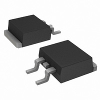
DIODE SCHOTTKY 30V 15A D2PAK
Manufacturer
ON Semiconductor
Series
SWITCHMODE™r
Datasheet
1.MBRB3030CTLG.pdf
(8 pages)
Specifications of MBRB3030CTLG
Voltage - Forward (vf) (max) @ If
440mV @ 15A
Current - Reverse Leakage @ Vr
2mA @ 30V
Current - Average Rectified (io) (per Diode)
15A
Voltage - Dc Reverse (vr) (max)
30V
Diode Type
Schottky
Speed
Fast Recovery =< 500ns, > 200mA (Io)
Diode Configuration
1 Pair Common Cathode
Mounting Type
Surface Mount
Package / Case
D²Pak, TO-263 (2 leads + tab)
Lead Free Status / RoHS Status
Lead free / RoHS Compliant
Reverse Recovery Time (trr)
-
Available stocks
Company
Part Number
Manufacturer
Quantity
Price
Company:

Part Number:
MBRB3030CTLG
Manufacturer:
ON
Quantity:
12 500
Part Number:
MBRB3030CTLG
Manufacturer:
ON/安森美
Quantity:
20 000


Suggested Method of Characterization
tested to failure using inductors ranging in value from 0.01
to 159 mH. The reverse voltage and current waveforms are
acquired to determine the exact energy seen by the device
and the inductive current decay time. At least 4 distinct
inductors and 5 to 10 devices per inductor are used to
generate the characteristic current versus time relationship.
This relationship when coupled with the application circuit
conditions, defines the SOA of the device uniquely for this
application.
Utilizing the UIS test circuit in Figure 10, devices are
Figure 11. Typical Voltage and Current UIS
INDUCTOR
CURRENT
Waveforms
TIME (s)
DUT
REVERSE
VOLTAGE
http://onsemi.com
MBRB3030CTL
5
Example Application
which is a 30 A (15 A per side) forward current, 35 V reverse
breakdown voltage rectifier. All parts were tested to
destruction at 25°C. The inductors used for the
characterization were 10, 3.0, 1.0 and 0.3 mH. The data
recorded from the testing were peak reverse current (Ip),
peak reverse breakdown voltage (BVR), maximum
withstand energy, inductance and inductor discharge time
(see Table 1). A plot of the Peak Reverse Current versus
Time at device destruction, as shown in Figure 12, was
generated. The area under the curve is the region of lower
reverse energy or lower stress on the device. This area is
known as the safe operating area or SOA.
120
100
80
60
40
20
The device used for this example was an MBR3035CT,
0
0
SAFE OPERATING AREA
Figure 12. Peak Reverse Current versus
0.0005 0.001 0.0015 0.002 0.0025
UIS CHARACTERIZATION CURVE
Time for DUT
TIME (s)
0.003 0.0035 0.004
Related parts for MBRB3030CTLG
Image
Part Number
Description
Manufacturer
Datasheet
Request
R

Part Number:
Description:
ON Semiconductor [VOLTAGE REGULATOR]
Manufacturer:
ON Semiconductor
Datasheet:
Part Number:
Description:
357-036-542-201 CARDEDGE 36POS DL .156 BLK LOPRO
Manufacturer:
ON Semiconductor
Datasheet:
Part Number:
Description:
357-036-542-201 CARDEDGE 36POS DL .156 BLK LOPRO
Manufacturer:
ON Semiconductor
Datasheet:
Part Number:
Description:
357-036-542-201 CARDEDGE 36POS DL .156 BLK LOPRO
Manufacturer:
ON Semiconductor
Datasheet:
Part Number:
Description:
357-036-542-201 CARDEDGE 36POS DL .156 BLK LOPRO
Manufacturer:
ON Semiconductor
Datasheet:
Part Number:
Description:
357-036-542-201 CARDEDGE 36POS DL .156 BLK LOPRO
Manufacturer:
ON Semiconductor
Datasheet:
Part Number:
Description:
357-036-542-201 CARDEDGE 36POS DL .156 BLK LOPRO
Manufacturer:
ON Semiconductor
Datasheet:
Part Number:
Description:
357-036-542-201 CARDEDGE 36POS DL .156 BLK LOPRO
Manufacturer:
ON Semiconductor
Datasheet:
Part Number:
Description:
357-036-542-201 CARDEDGE 36POS DL .156 BLK LOPRO
Manufacturer:
ON Semiconductor
Datasheet:
Part Number:
Description:
357-036-542-201 CARDEDGE 36POS DL .156 BLK LOPRO
Manufacturer:
ON Semiconductor
Datasheet:
Part Number:
Description:
357-036-542-201 CARDEDGE 36POS DL .156 BLK LOPRO
Manufacturer:
ON Semiconductor
Datasheet:
Part Number:
Description:
Manufacturer:
ON Semiconductor
Datasheet:
Part Number:
Description:
Manufacturer:
ON Semiconductor
Datasheet:
Part Number:
Description:
Manufacturer:
ON Semiconductor
Datasheet: