SI5515DC-T1-E3 Vishay, SI5515DC-T1-E3 Datasheet - Page 10
SI5515DC-T1-E3
Manufacturer Part Number
SI5515DC-T1-E3
Description
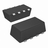
MOSFET N/P-CH 20V CHIPFET 1206-8
Manufacturer
Vishay
Series
TrenchFET®r
Specifications of SI5515DC-T1-E3
Fet Type
N and P-Channel
Fet Feature
Logic Level Gate
Rds On (max) @ Id, Vgs
40 mOhm @ 4.4A, 4.5V
Drain To Source Voltage (vdss)
20V
Current - Continuous Drain (id) @ 25° C
4.4A, 3A
Vgs(th) (max) @ Id
1V @ 250µA
Gate Charge (qg) @ Vgs
7.5nC @ 4.5V
Power - Max
1.1W
Mounting Type
Surface Mount
Package / Case
1206-8 ChipFET™
Transistor Polarity
N And P Channel
Continuous Drain Current Id
4.4A
Drain Source Voltage Vds
20V
On Resistance Rds(on)
32mohm
Rds(on) Test Voltage Vgs
4.5V
Threshold Voltage Vgs Typ
400mV
Lead Free Status / RoHS Status
Lead free / RoHS Compliant
Other names
SI5515DC-T1-E3TR
Available stocks
Company
Part Number
Manufacturer
Quantity
Price
Company:

Part Number:
SI5515DC-T1-E3
Manufacturer:
Vishay/Siliconix
Quantity:
32 095
Part Number:
SI5515DC-T1-E3
Manufacturer:
VISHY
Quantity:
20 000


INTRODUCTION
New Vishay Siliconix ChipFETs in the leadless 1206-8
package feature the same outline as popular 1206-8 resistors
and capacitors but provide all the performance of true power
semiconductor devices. The 1206-8 ChipFET has the same
footprint as the body of the LITTLE FOOTR TSOP-6, and can
be thought of as a leadless TSOP-6 for purposes of visualizing
board area, but its thermal performance bears comparison
with the much larger SO-8.
This technical note discusses the dual ChipFET 1206-8
pin-out, package outline, pad patterns, evaluation board
layout, and thermal performance.
PIN-OUT
Figure 1 shows the pin-out description and Pin 1 identification
for the dual-channel 1206-8 ChipFET device. The pin-out is
similar to the TSOP-6 configuration, with two additional drain
pins to enhance power dissipation and thus thermal
performance. The legs of the device are very short, again
helping to reduce the thermal path to the external heatsink/pcb
and allowing a larger die to be fitted in the device if necessary.
For package dimensions see the 1206-8 ChipFET package
outline drawing (http://www.vishay.com/doc?71151).
BASIC PAD PATTERNS
The basic pad layout with dimensions is shown in Application
Note 826, Recommended Minimum Pad Patterns With Outline
Drawing
(http://www.vishay.com/doc?72286). This is sufficient for low
power
semiconductor performance requires a greater copper pad
area, particularly for the drain leads.
Document Number: 71127
12-Dec-03
Dual-Channel 1206-8 ChipFETr Power MOSFET Recommended
dissipation
Access
D
1
D
1
MOSFET
Dual 1206-8 ChipFET
for
D
2
Pad Pattern and Thermal Performance
D
FIGURE 1.
2
Vishay Siliconix
applications,
S
1
G
1
S
2
but
G
MOSFETs,
2
power
The pad pattern with copper spreading shown in Figure 2
improves the thermal area of the drain connections (pins 5 and
6, pins 7 and 8) while remaining within the confines of the basic
footprint. The drain copper area is 0.0019 sq. in. or
1.22 sq. mm. This will assist the power dissipation path away
from the device (through the copper leadframe) and into the
board and exterior chassis (if applicable) for the dual device.
The addition of a further copper area and/or the addition of vias
to other board layers will enhance the performance still further.
An example of this method is implemented on the Vishay
Siliconix Evaluation Board described in the next section
(Figure 3).
THE VISHAY SILICONIX EVALUATION
BOARD FOR THE DUAL 1206-8
The dual ChipFET 1206-08 evaluation board measures 0.6 in
by 0.5 in. Its copper pad pattern consists of an increased pad
area around each of the two drain leads on the top-side—
approximately 0.0246 sq. in. or 15.87 sq. mm—and vias
added through to the underside of the board, again with a
maximized copper pad area of approximately the board-size
dimensions, split into two for each of the drains. The outer
package outline is for the 8-pin DIP, which will allow test
sockets to be used to assist in testing.
The thermal performance of the 1206-8 on this board has been
measured with the results following on the next page. The
testing included comparison with the minimum recommended
footprint on the evaluation board-size pcb and the industry
standard one-inch square FR4 pcb with copper on both sides
of the board.
FIGURE 2.
25 mil
18 mil
Footprint With Copper Spreading
26 mil
80 mil
Vishay Siliconix
10 mil
43 mil
www.vishay.com
AN812
1
Related parts for SI5515DC-T1-E3
Image
Part Number
Description
Manufacturer
Datasheet
Request
R

Part Number:
Description:
N/P-Ch 1206-8 ChipFET 20V 40/86mohm @ 4.5V
Manufacturer:
Vishay
Part Number:
Description:
Complementary 20-v D-s Mosfet
Manufacturer:
Vishay
Datasheet:
Part Number:
Description:
357-036-542-201 CARDEDGE 36POS DL .156 BLK LOPRO
Manufacturer:
Vishay
Datasheet:
Part Number:
Description:
357-036-542-201 CARDEDGE 36POS DL .156 BLK LOPRO
Manufacturer:
Vishay
Datasheet:
Part Number:
Description:
357-036-542-201 CARDEDGE 36POS DL .156 BLK LOPRO
Manufacturer:
Vishay
Datasheet:
Part Number:
Description:
357-036-542-201 CARDEDGE 36POS DL .156 BLK LOPRO
Manufacturer:
Vishay
Datasheet:
Part Number:
Description:
357-036-542-201 CARDEDGE 36POS DL .156 BLK LOPRO
Manufacturer:
Vishay
Datasheet:
Part Number:
Description:
357-036-542-201 CARDEDGE 36POS DL .156 BLK LOPRO
Manufacturer:
Vishay
Datasheet:
Part Number:
Description:
357-036-542-201 CARDEDGE 36POS DL .156 BLK LOPRO
Manufacturer:
Vishay
Datasheet:
Part Number:
Description:
357-036-542-201 CARDEDGE 36POS DL .156 BLK LOPRO
Manufacturer:
Vishay
Datasheet:
Part Number:
Description:
357-036-542-201 CARDEDGE 36POS DL .156 BLK LOPRO
Manufacturer:
Vishay
Datasheet:
Part Number:
Description:
357-036-542-201 CARDEDGE 36POS DL .156 BLK LOPRO
Manufacturer:
Vishay
Datasheet:
Part Number:
Description:
357-036-542-201 CARDEDGE 36POS DL .156 BLK LOPRO
Manufacturer:
Vishay
Datasheet:
Part Number:
Description:
357-036-542-201 CARDEDGE 36POS DL .156 BLK LOPRO
Manufacturer:
Vishay
Datasheet:
Part Number:
Description:
357-036-542-201 CARDEDGE 36POS DL .156 BLK LOPRO
Manufacturer:
Vishay
Datasheet: