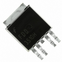
FDD3510H Fairchild Semiconductor, FDD3510H Datasheet - Page 10

FDD3510H
Manufacturer Part Number
FDD3510H
Description
IC MOSFET DUAL N/P 80V DPAK-4
Manufacturer
Fairchild Semiconductor
Series
PowerTrench®r
Specifications of FDD3510H
Fet Type
N and P-Channel
Fet Feature
Logic Level Gate
Rds On (max) @ Id, Vgs
80 mOhm @ 4.3A, 10V
Drain To Source Voltage (vdss)
80V
Current - Continuous Drain (id) @ 25° C
4.3A, 2.8A
Vgs(th) (max) @ Id
4V @ 250µA
Gate Charge (qg) @ Vgs
18nC @ 10V
Input Capacitance (ciss) @ Vds
800pF @ 40V
Power - Max
1.3W
Mounting Type
Surface Mount
Package / Case
DPak, TO-252 (4 leads + tab)
Configuration
Dual Common Drain Dual Source
Transistor Polarity
N-Channel
Resistance Drain-source Rds (on)
0.08 Ohm @ 10 V @ Q1
Drain-source Breakdown Voltage
80 V
Gate-source Breakdown Voltage
+/- 20 V
Continuous Drain Current
4.3 A @ Q1 or 2.8 A @ Q2
Power Dissipation
3100 mW
Maximum Operating Temperature
+ 150 C
Mounting Style
SMD/SMT
Minimum Operating Temperature
- 55 C
Lead Free Status / RoHS Status
Lead free / RoHS Compliant
Other names
FDD3510HTR
Available stocks
Company
Part Number
Manufacturer
Quantity
Price
Company:
Part Number:
FDD3510H
Manufacturer:
FSC
Quantity:
20 000
Part Number:
FDD3510H
Manufacturer:
ON/ه®‰و£®ç¾ژ
Quantity:
20 000
Highly Integrated Green-Mode PWM Controller
V
V
damage due to abnormal conditions. Once the V
voltage is over the over-voltage protection voltage
(V
disabled until the V
then start-up again. Over-voltage conditions are usually
caused by open feedback loops.
Thermal Protection
An NTC thermistor R
be connected from pin RT to ground. A constant current
I
expressed as V
(1.3V / R
such that V
(V
V
immediately after 100µs (t
Limited Power Control
The FB voltage increases every time the output of the
power supply is shorted or over-loaded. If the FB voltage
remains higher than a built-in threshold for longer than
t
turned off, the supply voltage V
© System General Corp.
Version 1.0.1 (IAO33.0083.B0)
D-OLP
RT
DD
RT
DD
DD-OVP
RTTH1
is output from pin RT. The voltage on RT pin can be
is less than 0.7V (V
over-voltage protection has been built in to prevent
, PWM output is turned off. As PWM output is
Over-Voltage Protection
), the PWM is turned off after 12ms (t
) and lasts for t
I
). At high ambient temperature, R
RT
RT
decreases. When V
= I
DD
RT
NTC
× (R
voltage drops below the UVLO,
RTTH2
D-VDDOVP
in series with a resistor R
D-OTP2
NTC
), PWM should be turned off
DD
+ Ra), in which I
).
, the PWM pulses are be
begins decreasing.
RT
is less than 1.05V
NTC
is smaller,
D-OTP1
RT
A
= 2 x
). If
can
DD
- 10 -
When V
the controller is totally shut down. V
the turn-on threshold voltage of 16V through the start-up
resistor until PWM output is restarted. This protection
feature is activated as long as the over-loading condition
persists. This prevents the power supply from overheating
due to over loading conditions.
Noise Immunity
Noise on the current sense or control signal may cause
significant
continuous-conduction mode. Slope compensation helps
alleviate this problem. Good placement and layout
practices should be followed. Avoiding long PCB traces
and component leads, locating compensation and filter
components near the SG6742, and increasing the power
MOS gate resistance improves performance.
DD
goes below the turn-off threshold (eg, 10.5V)
pulse
www.sg.com.tw • www.fairchildsemi.com
width
Product Specification
jitter,
September 24, 2007
DD
particularly
is charged up to
SG6742
in


