FDD3510H Fairchild Semiconductor, FDD3510H Datasheet - Page 9
FDD3510H
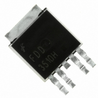
Manufacturer Part Number
FDD3510H
Description
IC MOSFET DUAL N/P 80V DPAK-4
Manufacturer
Fairchild Semiconductor
Series
PowerTrench®r
Specifications of FDD3510H
Fet Type
N and P-Channel
Fet Feature
Logic Level Gate
Rds On (max) @ Id, Vgs
80 mOhm @ 4.3A, 10V
Drain To Source Voltage (vdss)
80V
Current - Continuous Drain (id) @ 25° C
4.3A, 2.8A
Vgs(th) (max) @ Id
4V @ 250µA
Gate Charge (qg) @ Vgs
18nC @ 10V
Input Capacitance (ciss) @ Vds
800pF @ 40V
Power - Max
1.3W
Mounting Type
Surface Mount
Package / Case
DPak, TO-252 (4 leads + tab)
Configuration
Dual Common Drain Dual Source
Transistor Polarity
N-Channel
Resistance Drain-source Rds (on)
0.08 Ohm @ 10 V @ Q1
Drain-source Breakdown Voltage
80 V
Gate-source Breakdown Voltage
+/- 20 V
Continuous Drain Current
4.3 A @ Q1 or 2.8 A @ Q2
Power Dissipation
3100 mW
Maximum Operating Temperature
+ 150 C
Mounting Style
SMD/SMT
Minimum Operating Temperature
- 55 C
Lead Free Status / RoHS Status
Lead free / RoHS Compliant
Other names
FDD3510HTR
Available stocks
Company
Part Number
Manufacturer
Quantity
Price
Company:

Part Number:
FDD3510H
Manufacturer:
FSC
Quantity:
20 000
Part Number:
FDD3510H
Manufacturer:
ON/ه®‰و£®ç¾ژ
Quantity:
20 000


Highly Integrated Green-Mode PWM Controller
OPERATION DESCRIPTION
Start-up Current
For start-up, the HV pin is connected to the line input or
bulk capacitor through an external diode and resistor R
which are recommended as 1N4007 and 100KΩ. Typical
start-up current drawn from the HV pin is 1.2mA and it
charges the hold-up capacitor through the diode and
resistor. When the V
start-up current switches off. At this moment, the V
capacitor only supplies the SG6742 to keep the V
before the auxiliary winding of the main transformer to
carry on provide the operating current.
Operating Current
Operating current is around 4mA. The low operating
current enables better efficiency and reduces the
requirement of V
Green-Mode Operation
The patented green-mode function provides an off-time
modulation to reduce the switching frequency in
light-load and no-load conditions. The on-time is limited
for better abnormal or brownout protection. V
derived from the voltage feedback loop, is taken as the
reference. Once V
switching frequency is continuously decreased to the
minimum green mode frequency, around 22KHz.
Current Sensing / PWM Current Limiting
Peak-current-mode control is utilized to regulate output
voltage and provide pulse-by-pulse current limiting. The
switch current is detected by a sense resistor into the
SENSE pin. The PWM duty cycle is determined by this
current sense signal and V
the voltage on the SENSE pin reaches around V
(V
V
0.85V for output power limit.
Leading-Edge Blanking
Each time the power MOSFET is switched on, a turn-on
spike occurs on the sense-resistor. To avoid premature
termination of the switching pulse, a leading-edge
blanking time is built in. During this blanking period, the
current-limit comparator is disabled and it cannot switch
off the gate driver.
© System General Corp.
Version 1.0.1 (IAO33.0083.B0)
COMP
FB
–1.2)/4, a switch cycle is terminated immediately.
is internally clamped to a variable voltage around
DD
FB
hold-up capacitance.
DD
is lower than the threshold voltage,
capacitor level reaches V
FB
, the feedback voltage. When
FB
, which is
DD-ON
COMP
, the
HV
DD
DD
=
,
- 9 -
Under-Voltage Lockout (UVLO)
The turn-on and turn-off threshold are fixed internally at
16.5V/10.5V. During start-up, the hold-up capacitor must
be charged to 16.5V through the start-up resistor so that
IC is enabled. The hold-up capacitor continues to supply
V
winding of the main transformer. V
below 10.5V during this start-up process. This UVLO
hysteresis window ensures that hold-up capacitor is
adequate to supply V
Gate Output / Soft Driving
The SG6742 BiCMOS output stage is a fast totem pole
gate driver. Cross conduction is avoided to minimize heat
dissipation, increases efficiency, and enhances reliability.
The output driver is clamped by an internal 18V Zener
diode to protect power MOSFET transistors against
undesirable gate over voltage. A soft driving waveform is
implemented to minimize EMI.
Built-in Slope Compensation
The sensed voltage across the current-sense resistor is
used for peak-current-mode control and pulse-by-pulse
current limiting. Built-in slope compensation improves
stability or prevents sub-harmonic oscillation. SG6742
inserts a synchronized positive-going ramp at every
switching cycle.
Constant Output Power Limit
When the SENSE voltage, across the sense resistor Rs,
reaches the threshold voltage, around 0.9V, the output
GATE drive is turned off after a small delay, t
delay introduces additional current, proportional to
t
of the input voltage V
larger additional current and the output power limit is
higher than under low input line voltage. To compensate
this variation for wide AC input range, a sawtooth
power-limiter is designed to solve the unequal
power-limit problem. The power limiter is designed as a
positive ramp signal and is fed to the inverting input of the
OCP comparator. This results in a lower current limit at
high-line inputs than at low-line inputs.
PD
DD
•V
before the energy can be delivered from auxiliary
IN
/ L
P
. Since the delay is nearly constant, regardless
www.sg.com.tw • www.fairchildsemi.com
DD
IN
, higher input voltage results in a
during start-up.
Product Specification
September 24, 2007
DD
must not drop
SG6742
PD
. This
Related parts for FDD3510H
Image
Part Number
Description
Manufacturer
Datasheet
Request
R

Part Number:
Description:
Fairchild Semiconductor [IGBT MODULE]
Manufacturer:
Fairchild Semiconductor
Datasheet:

Part Number:
Description:
Discrete Semiconductor Modules
Manufacturer:
Fairchild Semiconductor
Part Number:
Description:
Discrete Semiconductor Modules
Manufacturer:
Fairchild Semiconductor
Part Number:
Description:
This N-Channel MOSFET is produced using Fairchild Semiconductor’s advanced Power Trench® process
Manufacturer:
Fairchild Semiconductor
Datasheet:
Part Number:
Description:
This N-Channel MOSFET is produced using Fairchild Semiconductor’s advanced Power Trench® process
Manufacturer:
Fairchild Semiconductor
Datasheet:
Part Number:
Description:
This N-Channel MOSFET is produced using Fairchild Semiconductor’s advanced PowerTrench® process
Manufacturer:
Fairchild Semiconductor
Datasheet:
Part Number:
Description:
This N-Channel MOSFET is produced using Fairchild Semiconductor’s advanced PowerTrench® process
Manufacturer:
Fairchild Semiconductor
Datasheet:
Part Number:
Description:
This N-Channel MOSFET is produced using Fairchild Semiconductor’s advanced Power Trench® process
Manufacturer:
Fairchild Semiconductor
Datasheet:
Part Number:
Description:
This N-Channel logic Level MOSFETs are produced using Fairchild Semiconductor‘s advanced Power Trench® process that has been special tailored to minimize the on-state resistance and yet maintain superior switching performance
Manufacturer:
Fairchild Semiconductor
Datasheet:
Part Number:
Description:
This N-Channel MOSFET is produced using Fairchild Semiconductor’s advanced Power Trench® process
Manufacturer:
Fairchild Semiconductor
Datasheet:
Part Number:
Description:
This N-Channel SyncFET™ is produced using Fairchild Semiconductor’s advanced PowerTrench® process
Manufacturer:
Fairchild Semiconductor
Datasheet:
Part Number:
Description:
This N-Channel SyncFET™ is produced using Fairchild Semiconductor’s advanced PowerTrench® process
Manufacturer:
Fairchild Semiconductor
Datasheet:
Part Number:
Description:
This N-Channel SyncFET™ is produced using Fairchild Semiconductor’s advanced PowerTrench® process
Manufacturer:
Fairchild Semiconductor
Datasheet:
Part Number:
Description:
This N-Channel logic Level MOSFETs are produced using Fairchild Semiconductor‘s advanced Power Trench® process that has been special tailored to minimize the on-state resistance and yet maintain superior switching performance
Manufacturer:
Fairchild Semiconductor
Datasheet:
Part Number:
Description:
This N-Channel MOSFET is produced using Fairchild Semiconductor’s advanced Power Trench® process that has been especially tailored to minimize the on-state resistance and yet maintain superior switching performance
Manufacturer:
Fairchild Semiconductor
Datasheet: