FDD3510H Fairchild Semiconductor, FDD3510H Datasheet - Page 2
FDD3510H
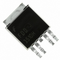
Manufacturer Part Number
FDD3510H
Description
IC MOSFET DUAL N/P 80V DPAK-4
Manufacturer
Fairchild Semiconductor
Series
PowerTrench®r
Specifications of FDD3510H
Fet Type
N and P-Channel
Fet Feature
Logic Level Gate
Rds On (max) @ Id, Vgs
80 mOhm @ 4.3A, 10V
Drain To Source Voltage (vdss)
80V
Current - Continuous Drain (id) @ 25° C
4.3A, 2.8A
Vgs(th) (max) @ Id
4V @ 250µA
Gate Charge (qg) @ Vgs
18nC @ 10V
Input Capacitance (ciss) @ Vds
800pF @ 40V
Power - Max
1.3W
Mounting Type
Surface Mount
Package / Case
DPak, TO-252 (4 leads + tab)
Configuration
Dual Common Drain Dual Source
Transistor Polarity
N-Channel
Resistance Drain-source Rds (on)
0.08 Ohm @ 10 V @ Q1
Drain-source Breakdown Voltage
80 V
Gate-source Breakdown Voltage
+/- 20 V
Continuous Drain Current
4.3 A @ Q1 or 2.8 A @ Q2
Power Dissipation
3100 mW
Maximum Operating Temperature
+ 150 C
Mounting Style
SMD/SMT
Minimum Operating Temperature
- 55 C
Lead Free Status / RoHS Status
Lead free / RoHS Compliant
Other names
FDD3510HTR
Available stocks
Company
Part Number
Manufacturer
Quantity
Price
Company:

Part Number:
FDD3510H
Manufacturer:
FSC
Quantity:
20 000
Part Number:
FDD3510H
Manufacturer:
ON/ه®‰و£®ç¾ژ
Quantity:
20 000


FDD3510H Rev.C
Electrical Characteristics
Off Characteristics
On Characteristics
Dynamic Characteristics
Switching Characteristics
BV
∆BV
I
I
V
r
g
C
C
C
R
t
t
t
t
Q
Q
Q
∆V
DSS
GSS
d(on)
r
d(off)
f
DS(on)
FS
GS(th)
iss
oss
rss
g
∆T
∆T
g(TOT)
gs
gd
Symbol
DSS
GS(th)
DSS
J
J
Drain to Source Breakdown Voltage
Breakdown Voltage Temperature
Coefficient
Zero Gate Voltage Drain Current
Gate to Source Leakage Current
Gate to Source Threshold Voltage
Gate to Source Threshold Voltage
Temperature Coefficient
Static Drain to Source On Resistance
Forward Transconductance
Input Capacitance
Output Capacitance
Reverse Transfer Capacitance
Gate Resistance
Turn-On Delay Time
Rise Time
Turn-Off Delay Time
Fall Time
Total Gate Charge
Gate to Source Charge
Gate to Drain “Miller” Charge
Parameter
T
J
= 25°C unless otherwise noted
V
V
I
I
V
V
V
V
V
V
V
V
I
I
I
I
V
V
V
Q1
V
Q2
V
f = 1MHz
Q1
V
V
Q2
V
V
Q1
V
Q2
V
D
D
D
D
D
D
GS
GS
GS
GS
GS
GS
GS
GS
DD
DD
DS
DS
GS
DS
DS
DD
GS
DD
GS
GS
GS
= 250µA, referenced to 25°C
= -250µA, referenced to 25°C
=250µA, V
= -250µA, V
= 250µA, referenced to 25°C
= -250µA, referenced to 25°C
= V
= V
= 10V, I
= 6.0V, I
= 10V, I
= -10V, I
= -4.5V, I
= -10V, I
= 10V, I
= -5V, I
= 40V, V
= -40V, V
= 64V, V
= -64V, V
= ±20V, V
= 40V, I
= 10V, R
= -40V, I
= -10V, R
= 10V, V
= -10V, V
DS
DS
Test Conditions
, I
, I
2
D
D
D
D
D
D
D
GS
GS
D
D
D
GEN
DD
D
GS
D
DD
= -2.8A
GEN
= 4.3A,
GS
GS
GS
DS
= 4.3A
= 4.3A, T
= 4.3A
= 250µA
= -250µA
= -2.8A, T
= -2.8A,
= 4.1A
= -2.8A
= -2.6A
= 0V, f = 1MHZ
= 0V
= 40V, I
= 0V, f = 1MHZ
= -40V, I
= 0V
= 0V
= 0V
= 0V
= 6Ω
= 6Ω
J
D
J
= 125°C
D
= 125°C
= 4.3A
= -2.8A
Type
Q1
Q2
Q1
Q2
Q1
Q2
Q1
Q2
Q1
Q2
Q1
Q2
Q1
Q2
Q1
Q2
Q1
Q2
Q1
Q2
Q2
Q1
Q2
Q1
Q2
Q1
Q2
Q1
Q2
Q1
Q2
Q1
Q2
Q1
Q2
Q1
Q2
Q1
Min
-80
-1.0
80
2.0
Typ
-67
-1.6
-6.7
600
660
121
153
184
259
84
2.6
4.6
6.8
1.7
7.2
2.3
1.9
3.2
2.9
64
70
15
56
50
27
25
16
25
13
14
7
6
2
3
2
5
±100
±100
Max
www.fairchildsemi.com
-3.0
152
190
224
322
800
880
4.0
-1
80
88
75
70
41
40
13
11
10
10
29
40
10
10
18
20
1
mV/°C
mV/°C
Units
mΩ
nC
nC
nC
µA
nA
nA
pF
pF
pF
ns
ns
ns
ns
Ω
V
V
S
Related parts for FDD3510H
Image
Part Number
Description
Manufacturer
Datasheet
Request
R

Part Number:
Description:
Fairchild Semiconductor [IGBT MODULE]
Manufacturer:
Fairchild Semiconductor
Datasheet:

Part Number:
Description:
Discrete Semiconductor Modules
Manufacturer:
Fairchild Semiconductor
Part Number:
Description:
Discrete Semiconductor Modules
Manufacturer:
Fairchild Semiconductor
Part Number:
Description:
This N-Channel MOSFET is produced using Fairchild Semiconductor’s advanced Power Trench® process
Manufacturer:
Fairchild Semiconductor
Datasheet:
Part Number:
Description:
This N-Channel MOSFET is produced using Fairchild Semiconductor’s advanced Power Trench® process
Manufacturer:
Fairchild Semiconductor
Datasheet:
Part Number:
Description:
This N-Channel MOSFET is produced using Fairchild Semiconductor’s advanced PowerTrench® process
Manufacturer:
Fairchild Semiconductor
Datasheet:
Part Number:
Description:
This N-Channel MOSFET is produced using Fairchild Semiconductor’s advanced PowerTrench® process
Manufacturer:
Fairchild Semiconductor
Datasheet:
Part Number:
Description:
This N-Channel MOSFET is produced using Fairchild Semiconductor’s advanced Power Trench® process
Manufacturer:
Fairchild Semiconductor
Datasheet:
Part Number:
Description:
This N-Channel logic Level MOSFETs are produced using Fairchild Semiconductor‘s advanced Power Trench® process that has been special tailored to minimize the on-state resistance and yet maintain superior switching performance
Manufacturer:
Fairchild Semiconductor
Datasheet:
Part Number:
Description:
This N-Channel MOSFET is produced using Fairchild Semiconductor’s advanced Power Trench® process
Manufacturer:
Fairchild Semiconductor
Datasheet:
Part Number:
Description:
This N-Channel SyncFET™ is produced using Fairchild Semiconductor’s advanced PowerTrench® process
Manufacturer:
Fairchild Semiconductor
Datasheet:
Part Number:
Description:
This N-Channel SyncFET™ is produced using Fairchild Semiconductor’s advanced PowerTrench® process
Manufacturer:
Fairchild Semiconductor
Datasheet:
Part Number:
Description:
This N-Channel SyncFET™ is produced using Fairchild Semiconductor’s advanced PowerTrench® process
Manufacturer:
Fairchild Semiconductor
Datasheet:
Part Number:
Description:
This N-Channel logic Level MOSFETs are produced using Fairchild Semiconductor‘s advanced Power Trench® process that has been special tailored to minimize the on-state resistance and yet maintain superior switching performance
Manufacturer:
Fairchild Semiconductor
Datasheet:
Part Number:
Description:
This N-Channel MOSFET is produced using Fairchild Semiconductor’s advanced Power Trench® process that has been especially tailored to minimize the on-state resistance and yet maintain superior switching performance
Manufacturer:
Fairchild Semiconductor
Datasheet: