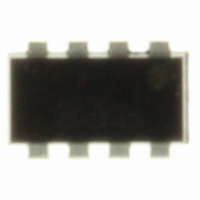
TPCF8402(TE85L) Toshiba, TPCF8402(TE85L) Datasheet

TPCF8402(TE85L)
Specifications of TPCF8402(TE85L)
Related parts for TPCF8402(TE85L)
TPCF8402(TE85L) Summary of contents
Page 1
... TOSHIBA Field Effect Transistor Silicon P, N Channel MOS Type (U-MOS IV / U-MOS III) Portable Equipment Applications Motor Drive Applications DC-DC Converter Applications • Low drain-source ON resistance : P Channel R • High forward transfer admittance : P Channel |Y • Low leakage current : P Channel I N Channel I • Enhancement-mode : P Channel V = − ...
Page 2
... Without a dot: [[Pb]]/INCLUDES > MCV With a dot: [[G]]/RoHS COMPATIBLE or [[G]]/RoHS [[Pb]] Please contact your TOSHIBA sales representative for details as to environmental matters such as the RoHS compatibility of Product. The RoHS is the Directive 2002/95/EC of the European Parliament and of the Council of 27 January 2003 on the restriction of the use of certain hazardous substances in electrical and electronic equipment. ...
Page 3
P-channel Electrical Characteristics Characteristics Gate leakage current Drain cut-off current Drain-source breakdown voltage Gate threshold voltage Drain-source ON resistance Forward transfer admittance Input capacitance Reverse transfer capacitance Output capacitance Rise time Turn-on time Switching time Fall time Turn-off time Total ...
Page 4
N-channel Electrical Characteristics Characteristics Gate leakage current Drain cut-off current Drain-source breakdown voltage Gate threshold voltage Drain-source ON resistance Forward transfer admittance Input capacitance Reverse transfer capacitance Output capacitance Rise time Turn-on time Switching time Fall time Turn-off time Total ...
Page 5
P-channel I – -3.5 -10 -6 -3 -0.4 -0.6 -0.2 Drain-source voltage – Common source -10 V Pulse test ...
Page 6
P-channel R – (ON) 150 120 -0.8A, -1.6A, -3. -4. -0.8A, -1.6A, -3. -10V 30 0 −80 − Ambient temperature Ta (°C) ...
Page 7
P-channel 1000 Single pulse 100 10 1 0.001 Safe operating area -100 I D max (pulsed Single pulse Ta = 25°C Curves must be derated linearly with increase in temperature. -0.1 -0.1 -1 ...
Page 8
N-channel I – 4.5 3.8 8.0 6 0.4 0.2 0.6 Drain-source voltage – Common source Pulse tset ...
Page 9
N-channel R – (ON) 120 Common source Pulse test 100 4. −80 − Ambient temperature Ta (°C) Capacitance – V 1000 100 ...
Page 10
N-channel 1000 Single Pulse 100 10 1 0.001 Safe operating area 100 I D max (Pulsed Single pulse Ta = 25°C Curves must be derated linearly with increase in temperature. 0.1 0.1 1 ...
Page 11
... Product shall not be used for or incorporated into any products or systems whose manufacture, use, or sale is prohibited under any applicable laws or regulations. • The information contained herein is presented only as guidance for Product use. No responsibility is assumed by TOSHIBA for any infringement of patents or any other intellectual property rights of third parties that may result from the use of Product. No license to any intellectual property right is granted by this document, whether express or implied, by estoppel or otherwise. • ...


