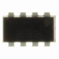
TPCF8402(TE85L) Toshiba, TPCF8402(TE85L) Datasheet - Page 3

TPCF8402(TE85L)
Manufacturer Part Number
TPCF8402(TE85L)
Description
MOSFET N/P-CH 30V 3.2A VS-8
Manufacturer
Toshiba
Datasheet
1.TPCF8402TE85LFM.pdf
(11 pages)
Specifications of TPCF8402(TE85L)
Fet Type
N and P-Channel
Fet Feature
Logic Level Gate
Rds On (max) @ Id, Vgs
50 mOhm @ 2A, 10V
Drain To Source Voltage (vdss)
30V
Current - Continuous Drain (id) @ 25° C
4A, 3.2A
Vgs(th) (max) @ Id
2V @ 1mA
Gate Charge (qg) @ Vgs
10nC @ 10V
Input Capacitance (ciss) @ Vds
470pF @ 10V
Power - Max
530mW
Mounting Type
Surface Mount
Package / Case
VS-8 (2-3U1B)
Lead Free Status / RoHS Status
Contains lead / RoHS non-compliant
Other names
TPCF8402TR
P-channel
Electrical Characteristics
Source-Drain Ratings and Characteristics
Gate leakage current
Drain cut-off current
Drain-source breakdown voltage
Gate threshold voltage
Drain-source ON resistance
Forward transfer admittance
Input capacitance
Reverse transfer capacitance
Output capacitance
Switching time
Total gate charge
(gate-source plus gate-drain)
Gate-source charge 1
Gate-drain (“miller”) charge
Drain reverse current
Forward voltage (diode)
Characteristics
Characteristics
Rise time
Turn-on time
Fall time
Turn-off time
Pulse (Note 1)
(Ta = 25°C)
V
V
R
Symbol
Symbol
(BR) DSS
(BR) DSX
DS (ON)
V
Q
I
I
C
I
C
|Y
C
Q
GSS
DSS
DRP
V
t
t
Q
DSF
oss
on
off
gs1
t
t
iss
rss
gd
th
fs
r
f
g
|
V
V
I
I
V
V
V
V
V
Duty ≤ 1%, t
V
I
I
D
D
D
DR
V
GS
DS
DS
GS
GS
DS
DS
DD
= −10 mA, V
= −10 mA, V
GS
= −3.2 A
3
= −3.2 A, V
(Ta = 25°C)
= ±16 V, V
= −30 V, V
= −10 V, I
= −4.5 V, I
= −10 V, I
= −10 V, I
= −10 V, V
≈ −24 V, V
−10
0 V
Test Condition
Test Condition
w
= 10 μs
D
D
D
GS
GS
GS
D
DS
GS
GS
GS
= −1 mA
= −1.6 A
= −1.6 A
⎯
= −1.6A
= 0 V
= 20 V
= 0 V
= 0 V
= 0 V
= 0 V, f = 1 MHz
= −10 V,
V
I
D
DD
= −1.6 A
≈ −15 V
V
OUT
−0.8
Min
−30
−15
Min
2.9
⎯
⎯
⎯
⎯
⎯
⎯
⎯
⎯
⎯
⎯
⎯
⎯
⎯
⎯
⎯
⎯
Typ.
Typ.
600
5.9
5.3
8.4
1.4
2.7
80
60
60
70
12
34
14
⎯
⎯
⎯
⎯
⎯
⎯
⎯
TPCF8402
2009-12-10
−12.8
−2.0
Max
Max
±10
−10
105
1.2
72
⎯
⎯
⎯
⎯
⎯
⎯
⎯
⎯
⎯
⎯
⎯
⎯
⎯
Unit
Unit
mΩ
nC
μA
μA
pF
ns
A
V
V
V
S


