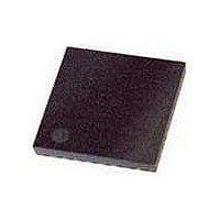
WM8983GEFL/RV Wolfson Microelectronics, WM8983GEFL/RV Datasheet - Page 80

WM8983GEFL/RV
Manufacturer Part Number
WM8983GEFL/RV
Description
Audio CODECs Mbl Multimedia CODEC w/ 1W Speaker Driver
Manufacturer
Wolfson Microelectronics
Specifications of WM8983GEFL/RV
Maximum Operating Temperature
+ 85 C
Mounting Style
SMD/SMT
Package / Case
QFN-32
Minimum Operating Temperature
- 25 C
Available stocks
Company
Part Number
Manufacturer
Quantity
Price
Company:
Part Number:
WM8983GEFL/RV
Manufacturer:
RENESAS
Quantity:
2 700
Part Number:
WM8983GEFL/RV
Manufacturer:
WOLFS0N
Quantity:
20 000
WM8983
DIGITAL AUDIO INTERFACES
w
Table 54 Unused Output Pin Bias Options
The audio interface has four pins:
The clock signals BCLK, and LRC can be outputs when the WM8983 operates as a master, or inputs
when it is a slave (see Master and Slave Mode Operation, below).
Five different audio data formats are supported:
All of these modes are MSB first. They are described in Audio Data Formats, below. Refer to the
Electrical Characteristic section for timing information.
MASTER AND SLAVE MODE OPERATION
The WM8983 audio interface may be configured as either master or slave. As a master interface
device the WM8983 generates BCLK and LRC and thus controls sequencing of the data transfer on
ADCDAT and DACDAT. To set the device to master mode register bit MS should be set high. In
slave mode (MS=0), the WM8983 responds with data to clocks it receives over the digital audio
interfaces.
AUDIO DATA FORMATS
In Left Justified mode, the MSB is available on the first rising edge of BCLK following an LRC
transition. The other bits up to the LSB are then transmitted in order. Depending on word length,
BCLK frequency and sample rate, there may be unused BCLK cycles before each LRC transition.
Figure 42 Left Justified Audio Interface (assuming n-bit word length)
L/ROUT2EN/
OUT3/4EN
•
•
•
•
•
•
•
•
•
0
0
0
0
1
1
ADCDAT: ADC data output
DACDAT: DAC data input
LRC: Data Left/Right alignment clock
BCLK: Bit clock, for synchronisation
Left justified
Right justified
I
DSP mode early
DSP mode late
2
S
OUT3BOOST/
OUT4BOOST/
SPKBOOST
0
0
1
1
0
1
VROI
X
X
0
1
0
1
1kΩ tie-off to AVDD1/2
30kΩ tie-off to AVDD1/2
1kΩ tie-off to 1.5xAVDD1/2
30kΩ tie-off to 1.5xAVDD1/2
Output enabled (DC level=AVDD1/2)
Output enabled (DC level=1.5xAVDD1/2)
OUTPUT CONFIGURATION
PD Rev 4.0 November 2006
Production Data
80


