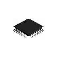
ispPAC-CLK5304S-01T48I Lattice, ispPAC-CLK5304S-01T48I Datasheet - Page 11

ispPAC-CLK5304S-01T48I
Manufacturer Part Number
ispPAC-CLK5304S-01T48I
Description
Clock Drivers & Distribution ISP 0 Delay Unv Fan- Out Buf-Sngl End I
Manufacturer
Lattice
Datasheet
1.ISPPAC-CLK5308S-01TN48C.pdf
(56 pages)
Specifications of ispPAC-CLK5304S-01T48I
Minimum Operating Temperature
- 40 C
Mounting Style
SMD/SMT
Maximum Operating Temperature
85 C
Package / Case
TQFP-48
Lead Free Status / RoHS Status
Lead free / RoHS Compliant
Available stocks
Company
Part Number
Manufacturer
Quantity
Price
Company:
Part Number:
ISPPAC-CLK5304S-01T48I
Manufacturer:
Lattice Semiconductor Corporation
Quantity:
10 000
Lattice Semiconductor
Performance Characteristics – PLL
f
t
t
t
t
f
f
V
f
t
t
t
tφ
tφ
DC
t
t
t
t
t
PSR
1. In PLL Bypass mode (PLL_BYPASS = HIGH), output will support frequencies down to 0Hz (divider chain is a fully static design).
2. See Figures 6 and 7 for output loads.
3. Input and outputs LVCMOS mode
4. Inserted feedback loop delay < 7ns
5. Measured with f
REF,
CLOCKHI,
CLOCKLO
RINP,
FINP
PFD
VCO
OUT
JIT
JIT
JIT(
PDBYPASS
PD_FOB
DELAY
LOCK
RELOCK
Symbol
DIV
DYN
ERR
(cc)
(per)
φ
)
f
FBK
Reference and feedback input
frequency range
Reference and feedback input
clock HIGH and LOW times
Reference and feedback input
rise and fall times
Phase detector input frequency
range
VCO operating frequency
Output divider range (Power of
2)
Output frequency range
Output adjacent-cycle jitter
(1000 cycle sample)
Output period jitter
(10000 cycle sample)
Reference clock to output jitter
(2000 cycle sample)
Static phase offset
Dynamic phase offset
Output duty cycle error
Reference clock to output
propagation delay
Reference to output propagation
delay in Non-Zero Delay Buffer
Mode
Reference to output delay with
internal feedback mode
PLL lock time
PLL relock time
Power supply rejection, period
jitter vs. power supply noise
OUT
= 100MHz, f
Parameter
5
4
VCO
3
1
= 400MHz, input and output interface set to LVCMOS.
5
5
Measured between 20% and 80%
levels
Fine Skew Mode
Coarse Skew Mode
f
f
f
PFD input frequency ≥100MHz
100MHz, Spread Spectrum
Modulation index = 0.5%
Output type LVCMOS 3.3V
f
V=1
V=1
V=1
From Power-up event
From RESET event
To same reference frequency
To different frequency
f
V
100kHz sinusoidal stimulus
PFD
PFD
PFD
OUT
IN
CCA
= f
≥ 100MHz
≥ 100MHz
≥ 100MHz
>100 MHz
OUT
= V
CCD
= 100MHz
Conditions
= V
11
CCO
modulated with
2
3
ispClock5300S Family Data Sheet
Min.
1.25
160
-40
2.5
2.5
47
8
8
1
5
Typ.
0.05
500
150
150
6.5
3.5
15
15
2
Max.
267
267
400
267
200
100
32
70
50
53
5
9
8
5
ps (RMS)
ps (RMS)
ps(RMS)
mV(p-p)
ps (p-p)
Units
MHz
MHz
MHz
MHz
MHz
ns
ns
ps
ps
ns
ns
ps
µs
µs
µs
µs
%


