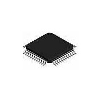
ispPAC-CLK5304S-01T48I Lattice, ispPAC-CLK5304S-01T48I Datasheet - Page 17

ispPAC-CLK5304S-01T48I
Manufacturer Part Number
ispPAC-CLK5304S-01T48I
Description
Clock Drivers & Distribution ISP 0 Delay Unv Fan- Out Buf-Sngl End I
Manufacturer
Lattice
Datasheet
1.ISPPAC-CLK5308S-01TN48C.pdf
(56 pages)
Specifications of ispPAC-CLK5304S-01T48I
Minimum Operating Temperature
- 40 C
Mounting Style
SMD/SMT
Maximum Operating Temperature
85 C
Package / Case
TQFP-48
Lead Free Status / RoHS Status
Lead free / RoHS Compliant
Available stocks
Company
Part Number
Manufacturer
Quantity
Price
Company:
Part Number:
ISPPAC-CLK5304S-01T48I
Manufacturer:
Lattice Semiconductor Corporation
Quantity:
10 000
Lattice Semiconductor
Detailed Description
PLL Subsystem
The ispClock5300S provides an integral phase-locked-loop (PLL) which may be used to generate output clock sig-
nals at lower, higher, or the same frequency as a user-supplied input reference signal. The core functions of the
PLL are an edge-sensitive phase detector, a programmable loop filter, and a high-speed voltage-controlled oscilla-
tor (VCO). Additionally, a set of programmable feedback dividers (V[0, 1, 2]) is provided to support the synthesis of
different output frequencies.
Phase/Frequency Detector
The ispClock5300S provides an edge-sensitive phase/frequency detector (PFD), which means that the device will
function properly over a wide range of input clock reference duty cycles. It is only necessary that the input refer-
ence clock meet specified minimum HIGH and LOW times (t
the PFD. The PFD’s output is of a classical charge-pump type, outputting charge packets which are then integrated
by the PLL‘s loop filter.
A lock-detection feature is also associated with the PFD. When the ispClock5300S is in a LOCKED state, the
LOCK output pin goes HIGH. The number of cycles required before asserting the LOCK signal in frequency-lock
mode can be set from 16 through 256.
When the lock condition is lost the LOCK signal will be de-asserted (Logic ‘0’) immediately.
Loop Filter: The loop filter parameters for each profile are automatically selected by the PAC-Designer software
depending on the following:
Spread Spectrum Support: The reference clock inputs of the ispClock5300S device are spread spectrum clock
tolerant. The tolerance limits are:
The ispClock5300S PLL has two modes of operation:
• Maximum VCO operating frequency
• Center spread ±0.125% to ±2%
• Down spread -0.25% to 0.5%
• 30-33kHz modulation frequency
• Spread Spectrum setting turned on - Spread Spectrum modulation is transferred from input to output with
• Spread Spectrum setting turned off - Spread Spectrum modulation transfer from input to output is attenu-
minimal attenuation.
ated. The extent of attenuation depends on the VCO operating frequency and the feedback divider value.
17
CLOCKHI,
t
CLOCKLO
ispClock5300S Family Data Sheet
) for it to be properly recognized by


