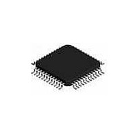
ispPAC-CLK5304S-01T48I Lattice, ispPAC-CLK5304S-01T48I Datasheet - Page 30

ispPAC-CLK5304S-01T48I
Manufacturer Part Number
ispPAC-CLK5304S-01T48I
Description
Clock Drivers & Distribution ISP 0 Delay Unv Fan- Out Buf-Sngl End I
Manufacturer
Lattice
Datasheet
1.ISPPAC-CLK5308S-01TN48C.pdf
(56 pages)
Specifications of ispPAC-CLK5304S-01T48I
Minimum Operating Temperature
- 40 C
Mounting Style
SMD/SMT
Maximum Operating Temperature
85 C
Package / Case
TQFP-48
Lead Free Status / RoHS Status
Lead free / RoHS Compliant
Available stocks
Company
Part Number
Manufacturer
Quantity
Price
Company:
Part Number:
ISPPAC-CLK5304S-01T48I
Manufacturer:
Lattice Semiconductor Corporation
Quantity:
10 000
Lattice Semiconductor
ispClock5300 Operating Configuration Summary
The following table summarizes the operating modes of the ispClock5300S.
Note:
Table 3. ispClock5300S Operating Modes
Thermal Management
In applications where a majority of the ispClock5300S’s outputs are active and operating at or near maximum out-
put frequency, package thermal limitations may need to be considered to ensure a successful design. Thermal
characteristics of the packages employed by Lattice Semiconductor may be found in the document Thermal Man-
agement which may be obtained at www.latticesemi.com.
The maximum current consumption of the digital and analog core circuitry for ispClock5312S is 150mA worst case
(I
MHz, both outputs in each bank enabled). This results in a total device dissipation:
With a maximum recommended operating junction temperature (T
maximum allowable ambient temperature (T
where Θ
The above analysis represents the worst-case scenario. Significant improvement in maximum ambient operating
temperature can be realized with additional cooling. Providing a 200 LFM (Linear Feet per Minute) airflow reduces
Θ
While it is possible to perform detailed calculations to estimate the maximum ambient operating temperature from
operating conditions, some simpler rule-of-thumb guidance can also be obtained through the derating curves
shown in Figure 25 which shows the maximum ambient operating temperature permitted when operating a given
number of output banks at the maximum output frequency.
Zero Delay Buffer Mode
Mixed Zero-Delay &
Non-Zero Delay Buffer Mode
Non-Zero Delay Fan-out Buffer
Mode 1
Non-Zero Delay Fan-out Buffer
Mode 2
CCD
JA
to 44°C/W for the 48 TQFP package.
• Whenever the input buffer is configured as differential input, the fan-out buffer paths become unavailable.
• Non-zero delay buffer for differential clock input is realized by using the PLL_BYPASS signal set to logical
• Output Skew control mechanism is available only to clock outputs sourced from PLL VCO.
+ I
Operating Mode
ispClock5300S
‘1’.
CCA
JA
= 48°C/W for the 48 TQFP package in still air and Θ
), and each of the output banks may draw up to 16mA worst case (LVCMOS 3.60V, CL=5pF, f
T
AMAX
Single Ended / Differential
Single Ended / Differential
Reference Input Clocks
= T
P
Single Ended Only
Single Ended Only
DMAX
JOP
- PD
= 3.60V x (6 x 16mA + 150mA) = 0.88W
AMAX
MAX
x Θ
) can be estimated as
JA
= 130°C - 0.88W x 48°C/W = 85°C
30
Only to Zero Delay
JA
Skew Control
Output Clocks
= 42°C/W for the 64 TQFP package in still air.
JOP
Yes
) of 130°C for an industrial grade device, the
No
No
ispClock5300S Family Data Sheet
Only to Clocks Sourced From
Frequency Divider
Only to Zero Delay
Bypassed PLL
Output Clock
Output Clocks
Yes
No
OUT
=100
(3)
(4)


