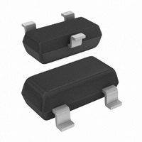
BSH103,215 NXP Semiconductors, BSH103,215 Datasheet - Page 5

BSH103,215
Manufacturer Part Number
BSH103,215
Description
MOSFET N-CH 30V 0.85A SOT23
Manufacturer
NXP Semiconductors
Datasheet
1.BSH103235.pdf
(12 pages)
Specifications of BSH103,215
Package / Case
SOT-23-3, TO-236-3, Micro3™, SSD3, SST3
Fet Type
MOSFET N-Channel, Metal Oxide
Fet Feature
Logic Level Gate
Rds On (max) @ Id, Vgs
400 mOhm @ 500mA, 4.5V
Drain To Source Voltage (vdss)
30V
Current - Continuous Drain (id) @ 25° C
850mA
Vgs(th) (max) @ Id
400mV @ 1mA
Gate Charge (qg) @ Vgs
2.1nC @ 4.5V
Input Capacitance (ciss) @ Vds
83pF @ 24V
Power - Max
540mW
Mounting Type
Surface Mount
Minimum Operating Temperature
- 55 C
Configuration
Single
Transistor Polarity
N-Channel
Resistance Drain-source Rds (on)
0.4 Ohm @ 4.5 V
Drain-source Breakdown Voltage
30 V
Gate-source Breakdown Voltage
+/- 8 V
Continuous Drain Current
0.85 A
Power Dissipation
500 mW
Maximum Operating Temperature
+ 150 C
Mounting Style
SMD/SMT
Lead Free Status / RoHS Status
Lead free / RoHS Compliant
Lead Free Status / RoHS Status
Lead free / RoHS Compliant, Lead free / RoHS Compliant
Other names
568-5013-2
934054713215
BSH103 T/R
BSH103 T/R
BSH103,215
934054713215
BSH103 T/R
BSH103 T/R
BSH103,215
Available stocks
Company
Part Number
Manufacturer
Quantity
Price
Company:
Part Number:
BSH103,215
Manufacturer:
TI
Quantity:
12 900
Part Number:
BSH103,215
Manufacturer:
NEXPERIA/安世
Quantity:
20 000
Philips Semiconductors
CHARACTERISTICS
T
1998 Feb 11
V
V
I
I
R
C
C
C
Q
Q
Q
Switching times
t
t
t
t
t
t
Source-drain diode
V
t
SYMBOL
j
DSS
GSS
d(on)
f
on
d(off)
r
off
rr
(BR)DSS
GSth
SD
= 25 C unless otherwise specified.
DSon
iss
oss
rss
N-channel enhancement mode
MOS transistor
G
GS
GD
drain-source breakdown voltage
gate-source threshold voltage
drain-source leakage current
gate leakage current
drain-source on-state resistance
input capacitance
output capacitance
reverse transfer capacitance
total gate charge
gate-source charge
gate-drain charge
turn-on delay time
fall time
turn-on switching time
turn-off delay time
rise time
turn-off switching time
source-drain diode forward
voltage
reverse recovery time
PARAMETER
V
V
V
V
V
V
V
V
V
V
V
I
V
T
V
T
V
I
V
I
V
I
V
I
V
I
V
I
V
I
D
D
D
D
D
D
D
S
amb
amb
GS
GS
GS
GS
GS
GS
GS
GS
GS
GS
GS
DD
DD
GS
GS
GS
GS
GS
GS
GD
= 0.5 A; T
= 0.5 A; R
= 0.5 A; R
= 0.5 A; R
= 0.5 A; R
= 0.5 A; R
= 0.5 A; R
= 0.5 A; di/dt = 100 A/ s
= 4.5 V; I
= 2.5 V; I
= 1.8 V; I
= 0; V
= 0; V
= 0; V
= 4.5 V; V
= 0 to 8 V; V
= 0 to 8 V; V
= 0 to 8 V; V
= 8 to 0 V; V
= 8 to 0 V; V
= 8 to 0 V; V
= 0; I
= 0; I
= V
= 0; V
= 8 V; V
= 15 V; I
= 15 V; I
= 25 C
= 25 C
DS
D
S
5
CONDITIONS
DS
DS
DS
; I
DS
= 0.5 A
= 10 A
amb
gen
gen
gen
gen
gen
gen
D
D
D
D
D
D
= 24 V; f = 1 MHz
= 24 V; f = 1 MHz
= 24 V; f = 1 MHz
= 24 V
DS
= 1 mA
DD
= 0.5 A;
= 0.5 A;
= 0.5 A
= 0.5 A
= 0.25 A
= 6
= 6
= 6
= 6
= 6
= 6
= 25 C
DD
DD
DD
DD
DD
DD
= 0
= 15 V;
= 15 V;
= 15 V;
= 15 V;
= 15 V;
= 15 V;
= 15 V;
30
0.4
MIN.
83
27
14
2100
95
670
2.5
3.5
6
20
7
27
25
TYP.
Product specification
100
0.4
0.5
0.6
1
MAX.
BSH103
100
V
V
nA
nA
pF
pF
pF
pC
pC
pC
ns
ns
ns
ns
ns
ns
V
ns
UNIT


