STW7N95K3 STMicroelectronics, STW7N95K3 Datasheet
STW7N95K3
Specifications of STW7N95K3
Available stocks


Related parts for STW7N95K3


STW7N95K3 Summary of contents
Page 1
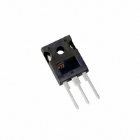
... Table 1. Device summary Order codes STF7N95K3 STP7N95K3 STW7N95K3 January 2009 STP7N95K3, STW7N95K3 7 7.2 A 150 W 7.2 A 150 W TO-220 Figure 1. Marking ...
Page 2
... Contents Contents 1 Electrical ratings . . . . . . . . . . . . . . . . . . . . . . . . . . . . . . . . . . . . . . . . . . . . 3 2 Electrical characteristics . . . . . . . . . . . . . . . . . . . . . . . . . . . . . . . . . . . . . 4 2.1 Electrical characteristics (curves) 3 Test circuits 4 Package mechanical data . . . . . . . . . . . . . . . . . . . . . . . . . . . . . . . . . . . . 10 5 Revision history . . . . . . . . . . . . . . . . . . . . . . . . . . . . . . . . . . . . . . . . . . . 14 2/ STF7N95K3, STP7N95K3, STW7N95K3 . . . . . . . . . . . . . . . . . . . . . . . . . . . . 6 ...
Page 3
... STF7N95K3, STP7N95K3, STW7N95K3 1 Electrical ratings Table 2. Absolute maximum ratings Symbol V Gate-source voltage GS I Drain current (continuous Drain current (continuous (2) I Drain current (pulsed Total dissipation at T TOT Max current during repetitive or single pulse I AR avalanche (pulse width limited Single pulse avalanche energy ...
Page 4
... Parameter Test conditions 100 MHz 760 760 f=1 MHz Gate DC Bias=0 Test signal level = 20 mV open drain V = 760 Figure 20) (see DSS DSS STF7N95K3, STP7N95K3, STW7N95K3 Min. Typ 950 =125 ° 100 µ 3.6 A 1.1 Min. Typ 1031 79 0 2 Max. Unit V 1 µ ...
Page 5
... STF7N95K3, STP7N95K3, STW7N95K3 Table 6. Switching times Symbol t Turn-on delay time d(on) t Rise time r t Turn-off-delay time d(off) t Fall time f Table 7. Source drain diode Symbol I Source-drain current SD (1) I Source-drain current (pulsed) SDM (2) V Forward on voltage SD t Reverse recovery time rr Q Reverse recovery charge ...
Page 6
... V (V) 100 DS Figure 5. AM01577v1 10µs 100µs 1ms 10ms V (V) 100 DS Figure 7. AM01578v1 10µs 100µs 1ms Tj=150°C 10ms Tc=25°C Single pulse 100 V (V) DS STF7N95K3, STP7N95K3, STW7N95K3 Thermal impedance for TO-220 Thermal impedance for TO-220FP Thermal impedance for TO-247 ...
Page 7
... STF7N95K3, STP7N95K3, STW7N95K3 Figure 8. Output characteristics Figure 10. Normalized B VDSS BV DSS (norm) 1.10 1.00 0.90 0.80 0.70 - Figure 12. Gate charge vs gate-source voltage Figure 13. Capacitance variations V GS (V) V =760 = =7 Figure 9. AM01579v1 (A) V =10V ( temperature Figure 11. Static drain-source on resistance AM01581v1 R DS(on) (Ω) 100 T (° ...
Page 8
... DS Figure 17. Normalized gate threshold voltage AM01587v1 V GS(th) (norm) T =25° =150° (A) SD AM01588v1 100 120 140 T (°C) J STF7N95K3, STP7N95K3, STW7N95K3 temperature 3.0 2.5 2.0 1.5 1.0 0 100 vs temperature 1.2 1.1 1.0 0.9 0.8 0.7 0.6 0.5 0.4 - 100 AM01582v1 T (° ...
Page 9
... STF7N95K3, STP7N95K3, STW7N95K3 3 Test circuits Figure 19. Switching times test circuit for resistive load D.U. Figure 21. Test circuit for inductive load switching and diode recovery times FAST L=100µH G D.U.T. DIODE Ω Figure 23. Unclamped inductive waveform Figure 20. Gate charge test circuit 3.3 2200 µ ...
Page 10
... Package mechanical data 4 Package mechanical data In order to meet environmental requirements, ST offers these devices in different grades of ECOPACK® packages, depending on their level of environmental compliance. ECOPACK® specifications, grade definitions and product status are available at: www.st.com. ECOPACK® trademark. 10/15 STF7N95K3, STP7N95K3, STW7N95K3 ...
Page 11
... STF7N95K3, STP7N95K3, STW7N95K3 Dim L20 L30 ∅P Q TO-220 mechanical data mm Min Typ Max 4.40 4.60 0.61 0.88 1.14 1.70 0.49 0.70 15.25 15.75 1.27 10 10.40 2.40 2.70 4.95 5.15 1.23 1.32 6.20 6.60 2.40 2. 3.50 3.93 16.40 28.90 3.75 3.85 2.65 2 ...
Page 12
... Package mechanical data Dim 12/15 TO-220FP mechanical data Dia STF7N95K3, STP7N95K3, STW7N95K3 7012510_Rev_J ...
Page 13
... STF7N95K3, STP7N95K3, STW7N95K3 Dim øP øR S TO-247 Mechanical data mm. Min. Typ 4.85 2.20 1.0 2.0 3.0 0.40 19.85 15.45 5.45 14.20 3.70 18.50 3.55 4.50 5.50 Package mechanical data Max. 5.15 2.60 1.40 2.40 3.40 0.80 20.15 15.75 14.80 4.30 3.65 5 ...
Page 14
... Revision history 5 Revision history Table 9. Document revision history Date 27-Jan-2009 14/15 Revision 1 First release STF7N95K3, STP7N95K3, STW7N95K3 Changes ...
Page 15
... STF7N95K3, STP7N95K3, STW7N95K3 Information in this document is provided solely in connection with ST products. STMicroelectronics NV and its subsidiaries (“ST”) reserve the right to make changes, corrections, modifications or improvements, to this document, and the products and services described herein at any time, without notice. All ST products are sold pursuant to ST’s terms and conditions of sale. ...