SSM6J53FE(TE85L,F) Toshiba, SSM6J53FE(TE85L,F) Datasheet
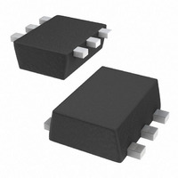
MOSFET P-CH 20V 1.8A ES6

SSM6J53FE(TE85L,F)

Manufacturer Part Number
SSM6J53FE(TE85L,F)
Description
MOSFET P-CH 20V 1.8A ES6
Manufacturer
Toshiba
Datasheet

Specifications of SSM6J53FE(TE85L,F)

Fet Type
MOSFET P-Channel, Metal Oxide
Fet Feature
Logic Level Gate
Rds On (max) @ Id, Vgs
136 mOhm @ 1A, 2.5V
Drain To Source Voltage (vdss)
20V
Current - Continuous Drain (id) @ 25° C
1.8A
Vgs(th) (max) @ Id
1V @ 1mA
Gate Charge (qg) @ Vgs
10.6nC @ 4V
Input Capacitance (ciss) @ Vds
568pF @ 10V
Power - Max
500mW
Mounting Type
Surface Mount
Package / Case
ES6
Lead Free Status / RoHS Status
Lead free / RoHS Compliant
Other names
SSM6J53FE(TE85LF)TR
○ High-Speed Switching Applications
○ Power Management Switch Applications
Absolute Maximum Ratings
Electrical Characteristics
Drain-Source breakdown voltage
Drain cut-off current
Gate leakage current
Gate threshold voltage
Forward transfer admittance
Drain-Source on-resistance
Input capacitance
Output capacitance
Reverse transfer capacitance
Switching time
Total gate charge
Gate-Source charge
Gate-Drain charge
Drain-Source forward voltage
Note 2: Pulse test
1.5 V drive
Suitable for high-density mounting due to compact package
Low on-resistance : R
Drain-Source voltage
Gate-Source voltage
Drain current
Drain power dissipation
Channel temperature
Storage temperature range
Note:
Note 1: Mounted on an FR4 board.
Using continuously under heavy loads (e.g. the application of
high temperature/current/voltage and the significant change in
temperature, etc.) may cause this product to decrease in the
reliability significantly even if the operating conditions (i.e.
operating temperature/current/voltage, etc.) are within the
absolute maximum ratings.
Please design the appropriate reliability upon reviewing the
Toshiba Semiconductor Reliability Handbook (“Handling
Precautions”/“Derating Concept and Methods”) and individual reliability data (i.e. reliability test report and
estimated failure rate, etc).
(25.4 mm × 25.4 mm × 1.6 t, Cu Pad: 645 mm
Characteristics
Characteristics
Turn-on time
Turn-off time
: R
: R
TOSHIBA Field Effect Transistor Silicon P Channel MOS Type
on
on
on
= 136 mΩ (max) (@V
= 204 mΩ (max) (@V
= 364 mΩ (max) (@V
Pulse
DC
(Ta = 25°C)
(Ta = 25°C)
SSM6J53FE
V
V
P
R
Symbol
Symbol
D
(BR) DSS
(BR) DSX
V
DS (ON)
V
V
I
I
C
T
C
|Y
C
Q
I
T
Q
DSS
GSS
GSS
V
(Note 1)
t
t
Q
I
DP
DSF
DS
stg
oss
on
off
D
ch
iss
rss
gd
th
gs
fs
g
|
GS
GS
GS
I
I
V
V
V
V
I
I
I
V
f = 1 MHz
V
V
V
V
I
= -2.5 V)
= -1.8 V)
= -1.5 V)
D
D
D
D
D
D
DS
GS
DS
DS
DS
DD
GS
DS
GS
= −1 mA, V
= −1 mA, V
= −1.0 A, V
= −1.0 A, V
= −0.1 A, V
= 1.8 A, V
−55~150
Rating
2
= −20 V, V
= −3 V, I
= −3 V, I
= −10 V, V
= −16 V, I
= ± 8 V, V
= −10 V, I
= 0 ~ −2.5 V, R
= − 4 V
)
-1.8
-3.6
500
150
-20
± 8
1
Test Condition
GS
D
D
GS
GS
GS
GS
GS
DS
D
DS
= −1 mA
= −0.9 A
GS
GS
= 0
= −0.9 A
= 0
= +8 V
= −2.5 V
= −1.8 V
= −1.5 V
= -1.8 A,
= 0
= 0
= 0
G
Unit
mW
°C
°C
V
V
A
= 4.7 Ω
(Note 2)
(Note 2)
(Note 2)
(Note 2)
(Note 2)
Weight: 7.0 mg (typ.)
JEDEC
JEITA
TOSHIBA
ES6
−0.3
Min
−20
−12
2.7
1,2,5,6 :Drain
3 :Gate
4 :Source
Typ.
10.6
122
137
568
1
5.4
7.4
3.3
0.8
2
3
95
75
67
29
39
SSM6J53FE
1.6±0.05
1.2±0.05
2-2N1A
Max
−1.0
−10
136
204
364
1.2
±1
2007-11-01
Unit : mm
Unit
6
5
4
μA
μA
nC
pF
ns
V
V
S
V

Related parts for SSM6J53FE(TE85L,F)

SSM6J53FE(TE85L,F) Summary of contents

Page 1

... TOSHIBA Field Effect Transistor Silicon P Channel MOS Type ○ High-Speed Switching Applications ○ Power Management Switch Applications • 1.5 V drive • Suitable for high-density mounting due to compact package • Low on-resistance : R = 136 mΩ (max) (@ 204 mΩ (max) (@ 364 mΩ (max) (@V on ...

Page 2

Switching Time Test Circuit (a) Test Circuit 0 IN − 2.5V 10 μ 4.7 Ω D.U. < < Common Source ...

Page 3

I – -3.5 -3 -2.5 V -2.5 -1 -1.5 VGS = -1 -0.5 Common Source Ta = 25° -0.5 -1 Drain - Source voltage – ...

Page 4

V – -0.8 Common Source -0 -0.6 -0.5 -0.4 -0.3 -0.2 -0.1 0 − 100 Ambient temperature Ta (°C) C – 5000 ...

Page 5

Single Pulse Mounted on FR4 board (25.4 mm × 25.4 mm × 1 Pad: 645 mm 100 10 1 0.001 0.01 Safe operating area - max (Pulsed ms max (Continuous) ...

Page 6

... Product shall not be used for or incorporated into any products or systems whose manufacture, use, or sale is prohibited under any applicable laws or regulations. • The information contained herein is presented only as guidance for Product use. No responsibility is assumed by TOSHIBA for any infringement of patents or any other intellectual property rights of third parties that may result from the use of Product. No license to any intellectual property right is granted by this document, whether express or implied, by estoppel or otherwise. • ...

Related keywords