NTZS3151PT1G ON Semiconductor, NTZS3151PT1G Datasheet - Page 4
NTZS3151PT1G
Manufacturer Part Number
NTZS3151PT1G
Description
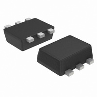
MOSFET P-CH 20V 860MA SOT-563
Manufacturer
ON Semiconductor
Datasheet
1.NTZS3151PT1G.pdf
(5 pages)
Specifications of NTZS3151PT1G
Fet Type
MOSFET P-Channel, Metal Oxide
Fet Feature
Logic Level Gate
Rds On (max) @ Id, Vgs
150 mOhm @ 950mA, 4.5V
Drain To Source Voltage (vdss)
20V
Current - Continuous Drain (id) @ 25° C
860mA
Vgs(th) (max) @ Id
1V @ 250µA
Gate Charge (qg) @ Vgs
5.6nC @ 4.5V
Input Capacitance (ciss) @ Vds
458pF @ 16V
Power - Max
170mW
Mounting Type
Surface Mount
Package / Case
SOT-563, SOT-6
Configuration
Single Quad Drain
Transistor Polarity
P-Channel
Resistance Drain-source Rds (on)
0.15 Ohm @ 4.5 V
Drain-source Breakdown Voltage
20 V
Gate-source Breakdown Voltage
+/- 8 V
Continuous Drain Current
0.86 A
Power Dissipation
170 mW
Maximum Operating Temperature
+ 150 C
Mounting Style
SMD/SMT
Minimum Operating Temperature
- 55 C
Lead Free Status / RoHS Status
Lead free / RoHS Compliant
Other names
NTZS3151PT1GOSTR
Available stocks
Company
Part Number
Manufacturer
Quantity
Price
Company:

Part Number:
NTZS3151PT1G
Manufacturer:
ON
Quantity:
242
Company:
Part Number:
NTZS3151PT1G
Manufacturer:
ON
Quantity:
30 000
Part Number:
NTZS3151PT1G
Manufacturer:
ON/安森美
Quantity:
20 000


ORDERING INFORMATION
†For information on tape and reel specifications, including part orientation and tape sizes, please refer to our Tape and Reel Packaging Specifi-
NTZS3151PT1G
NTZS3151PT5G
GATE−TO−SOURCE OR DRAIN−TO−SOURCE VOLTAGE (VOLTS)
1000
1000
cations Brochure, BRD8011/D.
900
800
700
600
500
400
300
200
100
100
10
0
1
10
1
Figure 9. Resistive Switching Time Variation
V
I
V
D
DD
GS
C
V
= −0.95 A
Device
RSS
DS
= −25 V
= −4.5 V
5
t
t
= 0 V
d(on)
d(off)
−V
t
t
Figure 7. Capacitance Variation
r
f
GS
R
vs. Gate Resistance
0
G
−V
, GATE RESISTANCE (W)
V
GS
TYPICAL PERFORMANCE CURVES
DS
C
OSS
= 0 V
5
10
10
15
(Pb−Free)
(Pb−Free)
SOT−563
SOT−563
Package
T
J
20
= 25°C
http://onsemi.com
C
ISS
100
25
4
5
4
3
2
1
0
0
1.2
1.0
0.8
0.6
0.4
0.2
(T
0
0.1
Q
J
GS
= 25°C unless otherwise noted)
V
T
Drain−to−Source Voltage vs. Total Charge
Figure 10. Diode Forward Voltage vs. Current
GS
J
−V
1
= 25°C
0.2
= 0 V
SD
Q
Q
−V
Figure 8. Gate−to−Source and
, SOURCE−TO−DRAIN VOLTAGE (VOLTS)
G
GD
, TOTAL GATE CHARGE (nC)
DS
0.3
2
4000 / Tape & Reel
8000 / Tape & Reel
0.4
QT
Shipping
3
0.5
4
0.6
I
T
D
J
0.7
= −0.77 A
= 25°C
5
−V
GS
0.8
6
30
25
20
15
10
5
0
0.9
Related parts for NTZS3151PT1G
Image
Part Number
Description
Manufacturer
Datasheet
Request
R

Part Number:
Description:
ON Semiconductor [VOLTAGE REGULATOR]
Manufacturer:
ON Semiconductor
Datasheet:
Part Number:
Description:
357-036-542-201 CARDEDGE 36POS DL .156 BLK LOPRO
Manufacturer:
ON Semiconductor
Datasheet:
Part Number:
Description:
357-036-542-201 CARDEDGE 36POS DL .156 BLK LOPRO
Manufacturer:
ON Semiconductor
Datasheet:
Part Number:
Description:
357-036-542-201 CARDEDGE 36POS DL .156 BLK LOPRO
Manufacturer:
ON Semiconductor
Datasheet:
Part Number:
Description:
357-036-542-201 CARDEDGE 36POS DL .156 BLK LOPRO
Manufacturer:
ON Semiconductor
Datasheet:
Part Number:
Description:
357-036-542-201 CARDEDGE 36POS DL .156 BLK LOPRO
Manufacturer:
ON Semiconductor
Datasheet:
Part Number:
Description:
357-036-542-201 CARDEDGE 36POS DL .156 BLK LOPRO
Manufacturer:
ON Semiconductor
Datasheet:
Part Number:
Description:
357-036-542-201 CARDEDGE 36POS DL .156 BLK LOPRO
Manufacturer:
ON Semiconductor
Datasheet:
Part Number:
Description:
357-036-542-201 CARDEDGE 36POS DL .156 BLK LOPRO
Manufacturer:
ON Semiconductor
Datasheet:
Part Number:
Description:
357-036-542-201 CARDEDGE 36POS DL .156 BLK LOPRO
Manufacturer:
ON Semiconductor
Datasheet:
Part Number:
Description:
357-036-542-201 CARDEDGE 36POS DL .156 BLK LOPRO
Manufacturer:
ON Semiconductor
Datasheet:
Part Number:
Description:
Manufacturer:
ON Semiconductor
Datasheet:
Part Number:
Description:
Manufacturer:
ON Semiconductor
Datasheet:
Part Number:
Description:
Manufacturer:
ON Semiconductor
Datasheet: