FDFS2P753Z Fairchild Semiconductor, FDFS2P753Z Datasheet
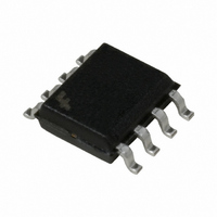
MOSFET P-CH 30V 3A 8-SOIC

FDFS2P753Z

Manufacturer Part Number
FDFS2P753Z
Description
MOSFET P-CH 30V 3A 8-SOIC
Manufacturer
Fairchild Semiconductor
Series
PowerTrench®r
Datasheet

Specifications of FDFS2P753Z

Fet Type
MOSFET P-Channel, Metal Oxide
Fet Feature
Diode (Isolated)
Rds On (max) @ Id, Vgs
115 mOhm @ 3A, 10V
Drain To Source Voltage (vdss)
30V
Current - Continuous Drain (id) @ 25° C
3A
Vgs(th) (max) @ Id
3V @ 250µA
Gate Charge (qg) @ Vgs
9.3nC @ 10V
Input Capacitance (ciss) @ Vds
455pF @ 10V
Power - Max
1.6W
Mounting Type
Surface Mount
Package / Case
8-SOIC (3.9mm Width)
Transistor Polarity
P Channel
Continuous Drain Current Id
3A
Drain Source Voltage Vds
30V
On Resistance Rds(on)
115mohm
Rds(on) Test Voltage Vgs
-10V
Threshold Voltage Vgs Typ
-2.1V
Rohs Compliant
Yes
Lead Free Status / RoHS Status
Lead free / RoHS Compliant
Other names
FDFS2P753ZTR

Available stocks

Company
Part Number
Manufacturer
Quantity
Price
Part Number:
FDFS2P753Z
Manufacturer:
FAIRCHILD/仙童
Quantity:
20 000
©2006 Fairchild Semiconductor Corporation
FDFS2P753Z Rev.A
MOSFET Maximum Ratings
Thermal Characteristics
Package Marking and Ordering Information
FDFS2P753Z
Integrated P-Channel PowerTrench
-30V, -3A, 115mΩ
Features
V
V
I
P
E
V
I
T
R
R
D
O
DS
GS
D
AS
RRM
J
θJA
θJC
Max r
Max r
V
Schottky and MOSFET incorporated into single power surface
mount SO-8 package
Electrically independent Schottky and MOSFET pinout for
design flexibility
RoHS Compliant
, T
V
F
Symbol
Device Marking
F
STG
FDFS2P753Z
< 500mV @ 1A
< 580mV @ 2A
DS(on)
DS(on)
SO-8
= 115mΩ at V
= 180mΩ at V
Drain to Source Voltage
Gate to Source Voltage
Drain Current -Continuous
Power Dissipation
Single Pulse Avalanche Energy
Schotty Repetitive Peak Reverse Voltage
Schotty Average Forward Current
Operating and Storage Junction Temperature Range
Thermal Resistance, Junction to Ambient
Thermal Resistance, Junction to Case
C
C
Pin 1
GS
GS
D
FDFS2P753Z
= -10V, I
= -4.5V, I
D
-Pulsed
Device
D
A
D
= -3.0A
= -1.5A
A
T
A
S
= 25°C unless otherwise noted
Parameter
G
Package
SO-8
®
1
MOSFET and Schottky Diode
General Description
The FDFS2P753Z combines the exceptional performance of
Fairchild's PowerTrench MOSFET technology with a very low
forward voltage drop Schottky barrier rectifier in an SO-8
package.
This device is designed specifically as a single package solution
for DC to DC converters. It features a fast switching, low gate
charge MOSFET with very low on-state resistance. The
independently connected Schottky diode allows its use in a
variety of DC/DC converter topologies.
Application
DC - DC Conversion
D
C
D
C
Reel Size
8
6
7
5
330mm
(Note 1a)
(Note 1a)
(Note 1a)
(Note 1a)
(Note 2)
(Note 1)
Tape Width
12mm
-55 to +150
Ratings
2
4
3
1
±25
-30
-16
1.6
-20
78
40
-3
-2
6
G
S
A
A
November 2006
www.fairchildsemi.com
2500 units
Quantity
Units
°C/W
mJ
°C
W
V
V
A
V
A
tm

Related parts for FDFS2P753Z

FDFS2P753Z Summary of contents

Page 1

... FDFS2P753Z ©2006 Fairchild Semiconductor Corporation FDFS2P753Z Rev.A ® MOSFET and Schottky Diode General Description = -3.0A The FDFS2P753Z combines the exceptional performance of D Fairchild's PowerTrench MOSFET technology with a very low = -1.5A D forward voltage drop Schottky barrier rectifier in an SO-8 package. This device is designed specifically as a single package solution for converters ...

Page 2

... Gate to Drain “Miller” Charge gd Drain-Source Diode Characteristics V Source to Drain Diode Forward Voltage SD t Reverse Recovery Time rr Q Reverse Recovery Charge rr Schottky Diode Characteristics I Reverse Leakage R V Forward Voltage F FDFS2P753Z Rev 25°C unless otherwise noted J Test Conditions I = -250µ -250µA, referenced to 25° -24V ...

Page 3

... R θJC a) 78°C/W when mounted on a 0.5in2 pad copper o 2: Starting 3mH 2A Pulse Test: Pulse Width < 300µs, Duty cycle < 2.0%. FDFS2P753Z Rev.A is determined by the user’s board design. θCA = 27V 10V 135°C/W when mounted on a minimun pad www.fairchildsemi.com ...

Page 4

... GS 1.4 1.2 1.0 0.8 0.6 -75 -50 - JUNCTION TEMPERATURE J Figure 3. Normalized On-Resistance vs Junction Temperature 16 PULSE DURATION = 80 µ s DUTY CYCLE = 0.5%MAX 150 GATE TO SOURCE VOLTAGE (V) GS Figure 5. Transfer Characteristics FDFS2P753Z Rev 25°C unless otherwise noted J µ -5V = -4.5V = -4V = -3. 100 125 150 ...

Page 5

... TIME IN AVALANCHE(ms) AV Figure 9. Unclamped Inductive Switching Capability OPERATION IN THIS 0.1 AREA MAY BE SINGLE PULSE LIMITED BY r DS(on MAX RATED 0.01 0 DRAIN to SOURCE VOLTAGE (V) Figure 11. Forward Bias Safe Operating Area FDFS2P753Z Rev 25°C unless otherwise noted -10V -15V 100us 1ms 10ms 100ms ...

Page 6

... Figure 13. Schottky Diode Forward Voltage 2 DUTY CYCLE-DESCENDING ORDER 0.5 0.2 0.1 0.05 0.1 0.02 0.01 0.01 SINGLE PULSE 0.005 - FDFS2P753Z Rev 25°C unless otherwise noted J 10 0.1 0.01 1E-3 1.2 1.6 2.0 Figure 14 RECTANGULAR PULSE DURATION (s) Figure 15. Transient Thermal Response Curve ...

Page 7

... PRODUCT STATUS DEFINITIONS Definition of Terms Datasheet Identification Advance Information Preliminary No Identification Needed Obsolete FDFS2P753Z Rev. A OCX™ SILENT SWITCHER OCXPro™ SMART START™ ® OPTOLOGIC SPM™ OPTOPLANAR™ ...

Related keywords