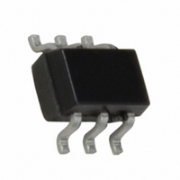
FDG332PZ Fairchild Semiconductor, FDG332PZ Datasheet - Page 2

FDG332PZ
Manufacturer Part Number
FDG332PZ
Description
MOSFET P-CH 20V 2.6A SC70-6
Manufacturer
Fairchild Semiconductor
Series
PowerTrench®r
Datasheet
1.FDG332PZ.pdf
(6 pages)
Specifications of FDG332PZ
Fet Type
MOSFET P-Channel, Metal Oxide
Fet Feature
Logic Level Gate
Rds On (max) @ Id, Vgs
95 mOhm @ 2.6A, 4.5V
Drain To Source Voltage (vdss)
20V
Current - Continuous Drain (id) @ 25° C
2.6A
Vgs(th) (max) @ Id
1.5V @ 250µA
Gate Charge (qg) @ Vgs
10.8nC @ 4.5V
Input Capacitance (ciss) @ Vds
560pF @ 10V
Power - Max
480mW
Mounting Type
Surface Mount
Package / Case
SC-70-6, SC-88, SOT-363
Configuration
Single Quad Drain
Transistor Polarity
P-Channel
Resistance Drain-source Rds (on)
0.095 Ohm @ 4.5 V
Drain-source Breakdown Voltage
20 V
Gate-source Breakdown Voltage
+/- 8 V
Continuous Drain Current
2.6 A
Power Dissipation
750 mW
Maximum Operating Temperature
+ 150 C
Mounting Style
SMD/SMT
Minimum Operating Temperature
- 55 C
Lead Free Status / RoHS Status
Lead free / RoHS Compliant
Other names
FDG332PZTR
Available stocks
Company
Part Number
Manufacturer
Quantity
Price
Company:
Part Number:
FDG332PZ
Manufacturer:
Fairchild Semiconductor
Quantity:
111 136
Company:
Part Number:
FDG332PZ
Manufacturer:
VISHAY
Quantity:
5 709
Part Number:
FDG332PZ
Manufacturer:
FAIRCHILD/ن»™ç«¥
Quantity:
20 000
©2008 Fairchild Semiconductor Corporation
FDG332PZ Rev.B1
Notes:
1. R
2. Pulse Test: Pulse Width < 300 s, Duty cycle < 2.0%.
Electrical Characteristics
Off Characteristics
On Characteristics
Dynamic Characteristics
Switching Characteristics
Drain-Source Diode Characteristics
BV
I
I
V
r
g
C
C
C
t
t
t
t
Q
Q
Q
I
V
t
Q
DSS
GSS
d(on)
r
d(off)
f
S
rr
DS(on)
the user's board design.
FS
BV
GS(th)
SD
iss
oss
rss
g
gs
gd
rr
V
Symbol
JA
DSS
T
T
GS(th)
DSS
J
J
is determined with the device mounted on a 1in
Maximum Continuous Drain-Source Diode Forward Current
Source to Drain Diode Forward Voltage
Reverse Recovery Time
Reverse Recovery Charge
Drain to Source Breakdown Voltage
Breakdown Voltage Temperature
Coefficient
Zero Gate Voltage Drain Current
Gate to Source Leakage Current
Gate to Source Threshold Voltage
Gate to Source Threshold Voltage
Temperature Coefficient
Static Drain to Source On Resistance
Forward Transconductance
Input Capacitance
Output Capacitance
Reverse Transfer Capacitance
Turn-On Delay Time
Rise Time
Turn-Off Delay Time
Fall Time
Total Gate Charge
Gate to Source Charge
Gate to Drain “Miller” Charge
Parameter
2
T
pad 2 oz copper pad on a 1.5 x 1.5 in. board of FR-4 material. R
J
= 25°C unless otherwise noted
a. 170°C/W when mounted on
and Maximum Ratings
a 1 in
2
pad of 2 oz copper .
I
I
V
V
V
I
V
V
V
V
V
V
V
V
V
V
V
I
D
D
D
F
DS
GS
GS
GS
GS
GS
GS
GS
DD
DS
DD
GS
GS
GS
= 2.6A, di/dt = 100A/ s
= -250 A, V
= -250 A, referenced to 25°C
= -250 A, referenced to 25°C
= -10V, V
= -16V, V
= -5V, I
= -10V, I
= -4.5V, V
= 0V, I
= ±8V, V
= V
= -4.5V, I
= -2.5V, I
= -1.8V, I
= -1.5V, I
= -4.5V, I
= -4.5V, R
2
DS
Test Conditions
, I
S
D
D
= -0.6A
D
DS
GS
= -250 A
D
D
D
D
D
= -2.6A
DD
GS
GS
GEN
= -2.6A,
= 0V
= -2.6A
= -2.2A
= -1.9A
= -1.0A
= -2.6A , T
= 0V, f = 1MHZ
= 0V
= 0V
= -10V, I
= 6
(Note 2)
D
J
= -2.6A
= 125°C
JC
is guaranteed by design while R
b. 260°C/W when mounted on
a minimum pad of 2 oz copper.
Min
-0.4
-20
-0.7
Typ
-0.7
117
147
100
420
-13
5.2
4.8
7.6
0.9
1.9
2.5
28
59
28
73
90
85
75
8
9
Max
10.8
-1.5
-0.6
-1.2
±10
115
160
330
133
560
115
115
CA
45
13
www.fairchildsemi.com
95
10
10
95
45
-1
is determined by
mV/°C
mV/°C
Units
m
nC
nC
nC
nC
pF
pF
pF
ns
ns
ns
ns
ns
V
A
V
V
S
A
A


