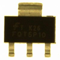
FQT5P10TF Fairchild Semiconductor, FQT5P10TF Datasheet - Page 2

FQT5P10TF
Manufacturer Part Number
FQT5P10TF
Description
MOSFET P-CH 100V 1A SOT-223
Manufacturer
Fairchild Semiconductor
Series
QFET™r
Type
Power MOSFETr
Datasheet
1.FQT5P10TF.pdf
(8 pages)
Specifications of FQT5P10TF
Fet Type
MOSFET P-Channel, Metal Oxide
Fet Feature
Standard
Rds On (max) @ Id, Vgs
1.05 Ohm @ 500mA, 10V
Drain To Source Voltage (vdss)
100V
Current - Continuous Drain (id) @ 25° C
1A
Vgs(th) (max) @ Id
4V @ 250µA
Gate Charge (qg) @ Vgs
8.2nC @ 10V
Input Capacitance (ciss) @ Vds
250pF @ 25V
Power - Max
2W
Mounting Type
Surface Mount
Package / Case
SOT-223 (3 leads + Tab), SC-73, TO-261
Configuration
Single
Transistor Polarity
P-Channel
Resistance Drain-source Rds (on)
1.05 Ohm @ 10 V
Forward Transconductance Gfs (max / Min)
1.4 S
Drain-source Breakdown Voltage
100 V
Gate-source Breakdown Voltage
+/- 30 V
Continuous Drain Current
1 A
Power Dissipation
2000 mW
Maximum Operating Temperature
+ 150 C
Mounting Style
SMD/SMT
Minimum Operating Temperature
- 55 C
Fall Time
30 ns
Rise Time
70 ns
Number Of Elements
1
Polarity
P
Channel Mode
Enhancement
Drain-source On-res
1.05Ohm
Drain-source On-volt
100V
Gate-source Voltage (max)
±30V
Operating Temp Range
-55C to 150C
Operating Temperature Classification
Military
Mounting
Surface Mount
Pin Count
3 +Tab
Package Type
SOT-223
Lead Free Status / RoHS Status
Lead free / RoHS Compliant
Other names
FQT5P10TF
FQT5P10TFTR
FQT5P10TFTR
Available stocks
Company
Part Number
Manufacturer
Quantity
Price
Company:
Part Number:
FQT5P10TF
Manufacturer:
Fairchild Semiconductor
Quantity:
47 158
Company:
Part Number:
FQT5P10TF
Manufacturer:
FSC
Quantity:
3 235
Part Number:
FQT5P10TF
Manufacturer:
ON/ه®‰و£®ç¾ژ
Quantity:
20 000
©2002 Fairchild Semiconductor Corporation
Electrical Characteristics
Notes:
1. Repetitive Rating : Pulse width limited by maximum junction temperature
2. L = 83mH, I
3. I
4. Pulse Test : Pulse width ≤ 300 s, Duty cycle ≤ 2%
5. Essentially independent of operating temperature
Off Characteristics
BV
/
I
I
I
On Characteristics
V
R
g
Dynamic Characteristics
C
C
C
Switching Characteristics
t
t
t
t
Q
Q
Q
Drain-Source Diode Characteristics and Maximum Ratings
I
I
V
trr
Qrr
Symbol
DSS
GSSF
GSSR
d(on)
r
d(off)
f
S
SM
SD
FS
B
GS(th)
SD
DS(on)
iss
oss
rss
g
gs
gd
VDSS
DSS
≤ -4.5A, di/dt ≤ 300A/ s, V
T
J
AS
Drain-Source Breakdown Voltage
Breakdown Voltage Temperature
Coefficient
Zero Gate Voltage Drain Current
Gate-Body Leakage Current, Forward
Gate-Body Leakage Current, Reverse
Gate Threshold Voltage
Static Drain-Source
On-Resistance
Forward Transconductance
Input Capacitance
Output Capacitance
Reverse Transfer Capacitance
Turn-On Delay Time
Turn-On Rise Time
Turn-Off Delay Time
Turn-Off Fall Time
Total Gate Charge
Gate-Source Charge
Gate-Drain Charge
Maximum Continuous Drain-Source Diode Forward Current
Maximum Pulsed Drain-Source Diode Forward Current
Drain-Source Diode Forward Voltage
Reverse Recovery Time
Reverse Recovery Charge
= -1.0A, V
DD
= -25V, R
DD
Parameter
≤ BV
G
= 25
DSS,
Starting T
Starting T
J
T
J
= 25°C
C
= 25°C
= 25°C unless otherwise noted
V
I
V
V
V
V
V
V
V
V
f = 1.0 MHz
V
R
V
V
V
V
dI
D
GS
DS
DS
GS
GS
DS
GS
DS
DS
DD
DS
GS
GS
GS
G
F
= -250 A, Referenced to 25°C
/ dt = 100 A/ s
= 25
= -100 V, V
= -80 V, T
= V
= -40 V, I
= -25 V, V
= -80 V, I
= 0 V, I
= -30 V, V
= 30 V, V
= -10 V, I
= -50 V, I
= -10 V
= 0 V, I
= 0 V, I
Test Conditions
GS
, I
D
S
S
D
= -250 A
D
D
= -1.0 A
= -4.5 A,
D
D
DS
C
= -250 A
GS
DS
= -0.5 A
= -4.5 A,
GS
= -0.5 A
= -4.5 A,
= 125°C
= 0 V
= 0 V
= 0 V,
= 0 V
(Note 4, 5)
(Note 4, 5)
(Note 4)
(Note 4)
-100
Min
-2.0
--
--
--
--
--
--
--
--
--
--
--
--
--
--
--
--
--
--
--
--
--
--
0.82
0.27
Typ
-0.1
190
1.4
6.3
1.7
3.0
70
18
70
12
30
85
--
--
--
--
--
--
--
--
--
9
Max
-100
1.05
100
-4.0
250
150
-1.0
-4.0
-4.0
-10
8.2
90
25
30
35
70
-1
--
--
--
--
--
--
--
Rev. B, August 2002
Units
V/°C
nC
nC
nC
nA
nA
pF
pF
pF
ns
ns
ns
ns
ns
V
V
S
A
A
V
A
A
C


